
Simple PWM inverter circuit diagram using PWM chip SG3524
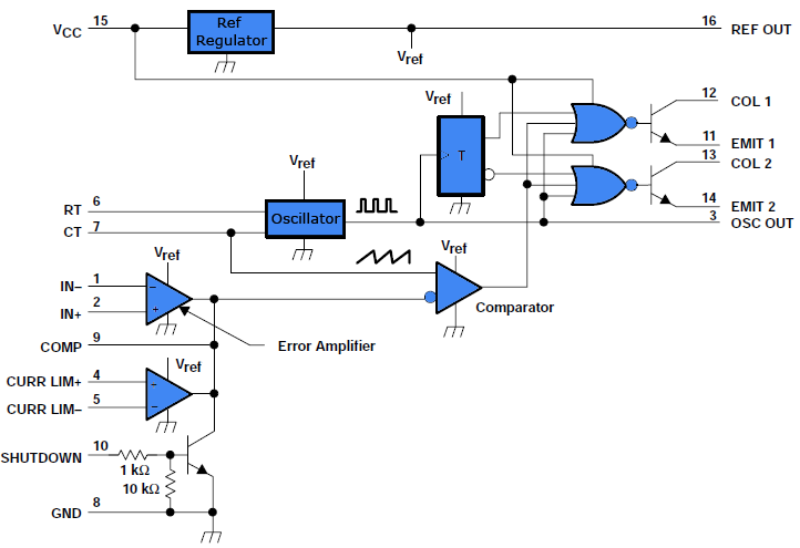
The SG3524 IC is designed for versatility in various applications, particularly in power electronics. Its ability to operate in both single-ended and push-pull configurations makes it suitable for driving transformers in inverter circuits, which are essential for converting DC power into AC power for various applications, including renewable energy systems and motor drives. The integrated error amplifier facilitates precise voltage regulation, ensuring that the output remains stable despite variations in input voltage or load conditions.
The programmable oscillator within the SG3524 allows for adjustment of the switching frequency, which is critical for optimizing the efficiency and performance of the inverter. The use of a timing capacitor (CT) not only influences the frequency but also plays a crucial role in determining the pulse width modulation characteristics, directly affecting the output waveform's quality.
The implementation of a pulse-steering flip-flop ensures that the outputs are complementary, thus enhancing the efficiency of the inverter by minimizing losses associated with simultaneous conduction of both transistors. This design feature is particularly important in high-power applications where heat dissipation and efficiency are paramount.
To achieve the desired output waveform, careful selection of external components, such as the resistor divider network for voltage sensing and the timing capacitor, is essential. This allows for fine-tuning of the PWM characteristics to match the requirements of specific AC loads. Overall, the SG3524-based inverter circuit exemplifies a robust solution for efficient DC to AC power conversion, with a range of applications in both consumer electronics and industrial systems.Here is a simple PWM dc to ac voltage inverter circuit based on IC SG 3524. The SG3524 IC chips is a fixed frequency PWM (Pulse Width Modulation) voltage regulator control circuit, with indifferent outputs for single ended or push pull applications. The SG3524 IC integrated circuit has all the functions necessary for the production of a regulating power supply, electrical inverteror switching regulator on a single chip. Moreover it can be used as the control element for high power output purposes. We know pulse width modulation PWM theory, i. e. a method of adjusting the width of the pulses in a pulse train relative to a control signal. If greater the control voltage, wider is the resultant pulses. Using a sinusoidal frequency as the control voltage for pulse width modulator circuits, it is likely to generate a high power waveform whose average voltage varies with the sine wave, which is suitable for driving ac loads. The complementary output allows either single-ended or push-pull application. Each device includes an on-chip regulator, error amplifier, programmable oscillator, pulse-steering flip-flop, two uncommitted pass transistors, a high-gain comparator, current-limiting and shutdown circuitry.
The inside reference voltage is divided on the outside by a resistor network to give a reference to inbuilt error amplifier. (External reference can also be used). The output is sensed by a subsequent resistor divider network and the error signal is amplified. This voltage is then compared with the linear voltage ramp at timing capacitor CT, thus producing a pulse width modulation (PWM) pulse.
The resultant PWM pulse from the comparator is passed to the corresponding output pass transistor (Q1, Q2 refer block diagram) using the pulse steering flip flop, which is synchronously toggled by the oscillator output. The oscillator output pulse also acts as an inhibiting pulse to make sure that both the transistors are never turned ON simultaneously.
The duration of this pulse is determined by the value of CT. When 11 of the IC pin goes high, lower transistor gets switched ON and current flows from the +12V source via the lower half of the transformer primary and sinks to the ground. 🔗 External reference
Related Circuits

This circuit allows any standard household bulb to shimmer or blink. It is compatible with incandescent lights up to 200 W and operates on standard 120 Vac. The circuit employs a silicon-controlled rectifier (SCR) to create the shimmering effect....

The interaction design for the singing pig was to have a different song start playing when a different wig is placed on the pig. The pig needed to stand by itself without being connected to anything else, and the...
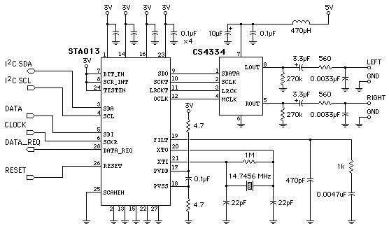
This page's mission is to assist in understanding the use of the STA013 MP3 decoder chip for designing an MP3 player. The player design outlined in subsequent pages utilizes the STA013, but this page aims to clarify the STA013...
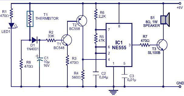
Various fire alarm circuits are discussed, featuring a new design that utilizes a thermistor and a timer. This circuit is straightforward and can be easily implemented. The thermistor exhibits low resistance at high temperatures and high resistance at low...

Writing about multiple circuits in Marx, an entire new set has been discovered, referred to as "the" Marx Generator. There are diagrams available, along with a useful quote: "The main advantage of the Marx circuit configuration over a more...
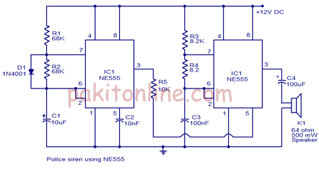
The circuit diagram of a police siren utilizes two NE555 timer integrated circuits (ICs), each configured as an astable multivibrator. It can operate with a power supply ranging from 6 to 15V DC and produces a loud sound. An...