
Simple structure hi-fi amplifier
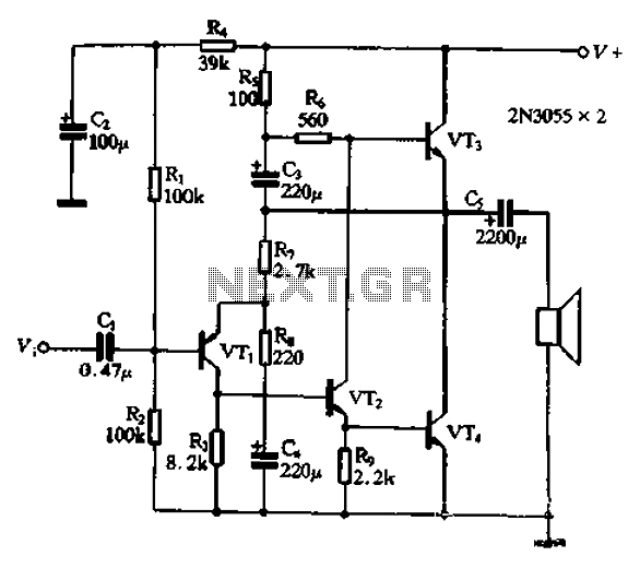
The circuit described utilizes a minimalist approach with four transistors, which are strategically arranged to achieve a high-fidelity amplification of the input signal. The PNP transistor (VT1) at the input stage is crucial for matching the input impedance, ensuring that the circuit can effectively interface with various signal sources without significant signal loss or distortion. The voltage amplification stage, facilitated by VT2, is configured in a common emitter mode, which is well-known for providing substantial voltage gain while also inverting the phase of the input signal.
Transistors VT3 and VT4 form a complementary push-pull output stage, which is essential for driving loads efficiently. This configuration allows for improved linearity and reduced distortion in the output signal, making it suitable for high-quality audio applications. The negative feedback loop, established through resistors R7 and R, plays a vital role in stabilizing the gain of the amplifier. The gain equation provided indicates that the circuit can be fine-tuned by adjusting the values of R7 and R, thereby allowing for versatility in various applications.
The bootstrap capacitor C3 enhances the amplifier's performance by improving the frequency response and stability, particularly at higher frequencies. Additionally, the isolation resistor R6 helps to prevent unwanted interactions between different stages of the circuit, ensuring that each transistor operates within its optimal range. Overall, this circuit design exemplifies a well-engineered amplifier capable of delivering high-fidelity audio output with minimal distortion, making it suitable for demanding audio applications. Circuit shown in Figure 240 of the circuit structure is very simple, with only four transistors to achieve circuit from input voltage put large, inverted, and promote the whole process of the amplifier, and a high technical indicators circuit, is an excellent high-fidelity power discharge path. VTi for the input stage, the use of a PNP transistor input stage and both impedance matching function, VTz voltage amplification stage and both CE and inverted push function, VT3 and VT4 constitute complementary push-pull amplifier output stage O R7, and R Pat negative feedback loop and determine the circuit gain: Av-R7 cuddle 8-2.7/0.22, together 21dBo bootstrap capacitor C3, R6 for the isolation resistance.
Related Circuits
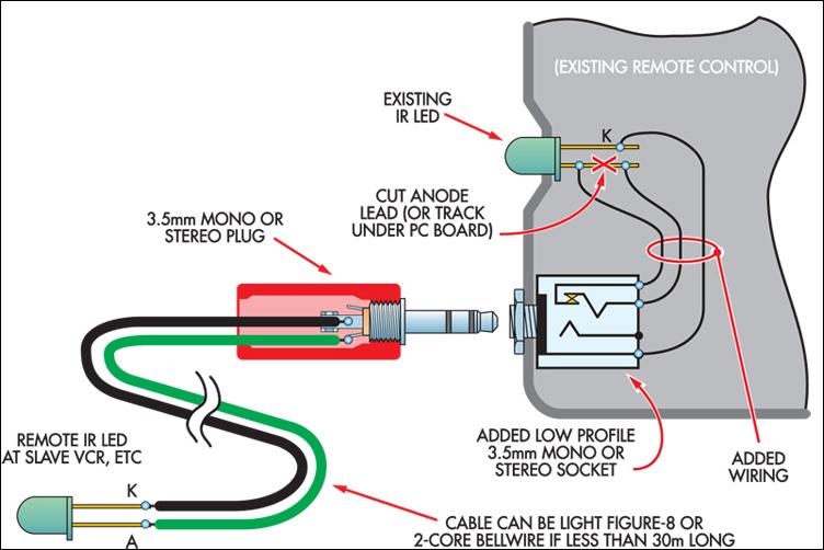
This ultra-simple remote control extender is ideal for use with a hidden video recorder. The recorder is a Panasonic NV-SD200 and is employed as part of a camera surveillance system. A PICAXE-08-based circuit detects events and controls the recorder....
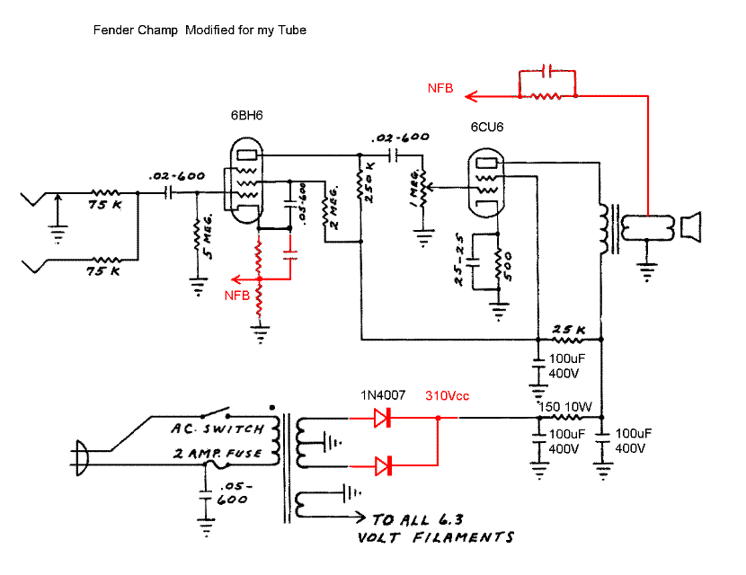
A collection of valves has been salvaged from an old television that was destined for scrap. Among these components, the 6CU6 valve, which is used for horizontal deflection, has been recovered along with a double valve. The 6CU6 is a...
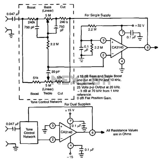
This circuit utilizes the high slew rate, high input impedance, and high output-voltage capability of the CA3140 BiMOS operational amplifier. It also offers mid-band unity gain using standard linear potentiometers. The circuit design leverages the characteristics of the CA3140 BiMOS...
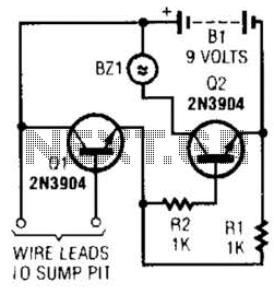
A common collector amplifier drives a 2N3904 switch to sound alarm BZ1. The wire leads to a water sensor or sump pit, level switch, etc. It is used to allow the alarm to operate and be mounted in a...

To create a telephone ring monitor, it is sufficient to connect a resistor in series with a bulb and plug it into a main outlet. The resistance value of this resistor may vary depending on the type of bulb...
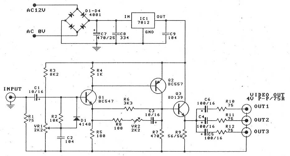
This is a video amplifier circuit or video splitter circuit, designed to strengthen video signals. It compensates for signal loss and is... The video amplifier circuit serves as a crucial component in video signal distribution systems, ensuring that the integrity...