
Simplest Solid State Tesla Switch
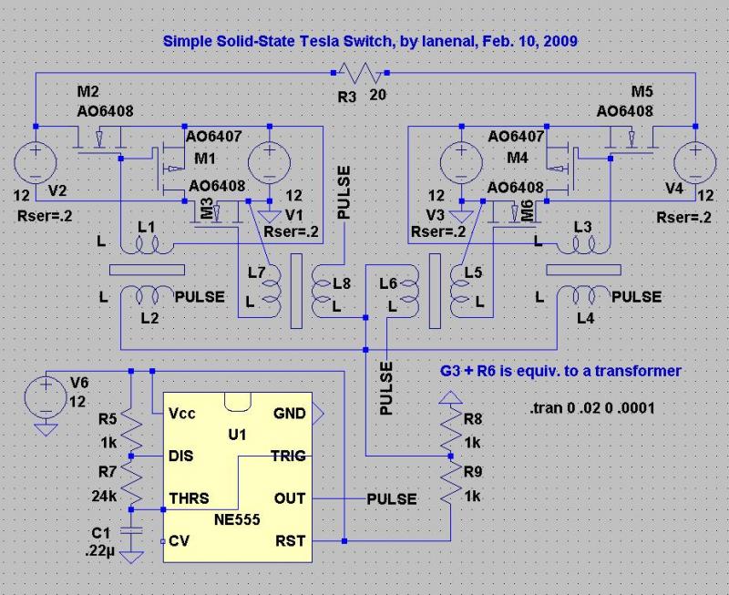
This circuit configuration is notable for its simplicity and efficiency, particularly in applications requiring precise control over switching elements. The use of a 555 timer in astable mode allows for the generation of a square wave signal, which can be adjusted for frequency and duty cycle to suit specific operational requirements. The voltage divider arrangement for V6 ensures that the voltage levels are appropriately set for the subsequent stages of the circuit, facilitating reliable transistor operation.
The replacement of JBT transistors with MOSFETs is advantageous due to the inherent characteristics of MOSFETs, which include higher switching speeds and reduced power loss during operation. The absence of diodes for switching further simplifies the design, minimizing component count and potential failure points. The voltage-dependent current source and resistor combination effectively emulate transformer action, enabling the circuit to handle varying load conditions without significant performance degradation.
The LTspice simulation results provide valuable insights into the circuit's performance, particularly the current behavior through the load resistor R3. It is crucial to include the capacitors at the load in practical implementations, as they play a vital role in stabilizing voltage and filtering high-frequency noise, thus enhancing overall circuit reliability.
The proposed 30V step-up voltage regulator is a critical component for driving the MOSFETs, ensuring that they operate within their optimal voltage range. The choice of using an iron dust or ferrite core for the regulator indicates a focus on efficiency and compactness in the design. The 555 timer's requirement for a 30V peak-to-peak output emphasizes the importance of ensuring that the switching transistors are adequately driven to prevent issues such as delayed switching or incomplete turn-on, which could lead to inefficiencies or circuit failure.
Overall, this circuit design exemplifies a well-thought-out approach to achieving efficient power management and control in electronic applications, making it suitable for a variety of uses in both experimental and practical scenarios.This circuit should be the easiest to tune as well (Reason: when the pulse is at 6V, all transistors should be open switch, so logically, there will never be battery shorts). The pulse voltage source V5 can be replaced by a 555 astable circuit. V6 can be obtained by using an equal voltage divider (two 5K resisters, for example) sharing the same power as the 555 circuit.
All the JBT transistors can be replaced with equiv. MOSFETs. I used voltage dependent current source and a resistor to mimick the behavior of a transformer. You can use 4 transformers instead in your implementation (MOSFETs are probably better than JBTs, I am affraid, as MOSFETs have no gate current). I used no diodes for switching purpose in this circuit. LTspice simulation is performed and the plot of the current over the load R3 is given below (I omitted the two capacitors at each end of the load R3 for the sake of simulation, in your implementation, you should include them).
This circuit should be the easiest to tune as well (Reason: when the pulse is at 6V, all transistors should be open switch, so logically, there will never be battery shorts).
The pulse voltage source V5 can be replaced by a 555 astable circuit. V6 can be obtained by using an equal voltage divider (two 5K resisters, for example) sharing the same power as the 555 circuit. All the JBT transistors can be replaced with equiv. MOSFETs. I used voltage dependent current source and a resistor to mimick the behavior of a transformer.
You can use 4 transformers instead in your implementation (MOSFETs are probably better than JBTs, I am affraid, as MOSFETs have no gate current).
I used no diodes for switching purpose in this circuit. LTspice simulation is performed and the plot of the current over the load R3 is given below (I omitted the two capacitors at each end of the load R3 for the sake of simulation, in your implementation, you should include them). The mosfets require a low power 30v step up voltage regulator which you can probably build yourself, using a iron dust or ferrite core & a single mosfet switching circuit.
The 555 timer is powered off 12 volts dc, however the output must be increased to 30 volts peak to peak to switch the npn & pnp transistor on & off properly.
Related Circuits
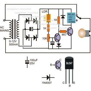
This circuit diagram illustrates a light-activated switch utilizing the National Semiconductor comparator IC LM311 and a light-dependent resistor (LDR). The configuration is based on a voltage comparator circuit centered around IC1. The non-inverting input of IC1 receives a reference...
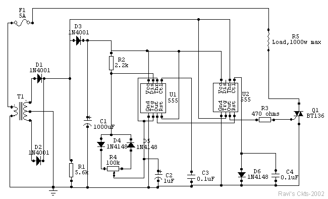
The circuit is constructed using two 555 timer integrated circuits, designated as U1 and U2. U1 is configured as a variable duty cycle oscillator with a fixed time period of approximately 0.1 seconds. The duty cycle can be adjusted...
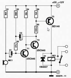
This sound-activated switch allows for control through sound, which can be beneficial not only in robotics but also in home automation applications. The sound-activated switch operates by detecting specific sound frequencies or patterns, typically using a microphone or a sound...
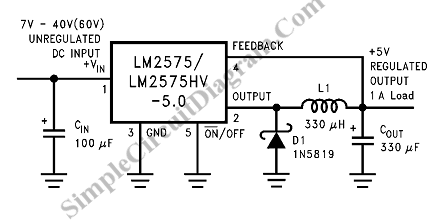
Switching Regulator for High Power Efficiency. When it is necessary to convert a high voltage to a significantly lower voltage, a switching regulator is the optimal choice. A switching regulator is an essential component in modern power management systems, particularly...
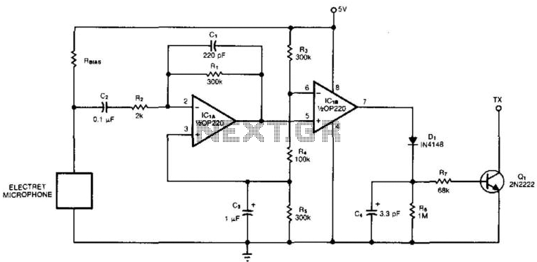
An electret microphone feeds a bandpass filter circuit (IC1A), which subsequently drives a comparator. This comparator activates Q1, a switch that conducts when audio signals from IC1B cause D1, C4, R6, and R7 to bias it ON. The circuit begins...
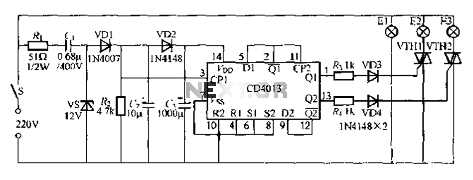
Figure 296 illustrates a control circuit that utilizes a switch (S) to manage three lamps (E1, E2, and E3) in a lighting system, suitable for controlling a chandelier in a living room. When the switch is off, all lights...