
SiPM Amplifier

The silicon photomultiplier (SiPM) system, integrated with an analog electronics board for signal amplification, represents a sophisticated approach to detecting and processing light signals. The amplifier circuit is critical for ensuring the accurate readout of signals from the SiPM, which is essential for applications such as particle detection and imaging. The integration of a MATLAB model allows for extensive simulation of the amplifier's performance, enabling the analysis of gain characteristics and operational parameters.
The amplifier circuit's design is based on a combination of theoretical and practical insights, where the initial schematic provided by Photonique serves as a foundation. The adjustments made to the resistor values and the introduction of a load resistor are crucial for achieving optimal performance. The choice of a 50-ohm load resistor is particularly relevant in ensuring impedance matching, which is vital for minimizing signal reflections and maximizing power transfer.
The linearized model developed in MATLAB is composed of twenty-four equations, representing a comprehensive analysis of the circuit's behavior. The four input parameters—input current, bias voltage, power voltage, and frequency—are essential for understanding the amplifier's response and tuning its performance. The ability to vary the power voltage between four and nine volts provides flexibility in adjusting the gain, which is a critical aspect of amplifier design.
The observations made regarding the amplifier's transimpedance gain highlight its significance in translating input current variations into output voltage changes. The linear relationship observed when varying the input current suggests a well-designed amplifier capable of maintaining a stable gain across a range of operating conditions. However, the limitations identified in high-frequency response necessitate further investigation and optimization.
The incorporation of capacitive effects and the modeling of SiPM discharge dynamics are essential steps in refining the amplifier design. By addressing the input impedance challenges, the overall performance of the amplifier can be enhanced, leading to faster signal processing capabilities. This is particularly important for applications requiring rapid detection and analysis of transient signals.
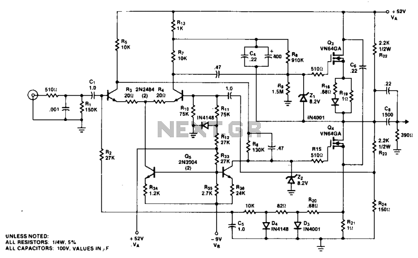
In summary, the integration of advanced modeling techniques with practical circuit design principles is crucial for developing effective SiPM amplifier systems. Ongoing optimization efforts will continue to enhance the performance and reliability of these systems in various applications.The silicon photomultipliers (SiPM) we are using in our experiment were purchased from Photonique. Photonique also supplies analog electronics boards to amplify the signals from the SiPMs. This page discusses the analysis and modeling of the amplifier circuit as well as design of the amplifier suitable for the readout of the tagger microscope. Th e amplifier circuit diagram shown below was developed through combining the diagram supplied by Photonique (lacking component values, and having several extra components) and the physical circuit (having most components labeled). We developed a model for this circuit in MATLAB to simulate its behavior and study various parameters, especially gain as a function of power voltage.
The Photonique documentation claims that the power voltage can be varied between four and nine volts in order to tune the gain of the amplifier. The MATLAB model is a linearized system of twenty-four equations, with the voltages and currents on the circuit being the twenty-four unknowns.
There are four input parameters: input current (Iin, in amps), the bias voltage (Vb, in volts), the power voltage (Vc, in volts), and the frequency (f, in hertz). The resistor values are mostly the same as the ones given for the above diagram, but some were changed to fit the model to actual data.
We also add a load resistor from Vout to GND, with a value of 50 ©. The transistors are described by a series of parameters from the Gummel-Poon SPICE model, and we included our best guesses of the capacitor values. We ran simulations of the MATLAB model while varying the input parameters to generate data on how the amplifier responds to each input.
We used as a baseline test the inputs Vb = 20V, Vc = 5V, f = 100MHz, and Iin = 1mA, then varied one parameter at a time to generate responses. Varying the input current from 0 to 2A results in a clean straight line that intersects the origin. Thus we can say that the amplifier has a transimpedance gain (programmable based on input parameters; in particular Vc) and no DC bias.
One of the principal limitations of this model turned out to be its inability to predict high-frequency behavior. Though the bandwidth inherent in the transistors themselves (4-5GHz) was not explicitly in the model, the low-pass behavior due to source capacitance and amplifier input impedance should appear in the solutions naturally.
It turned out that the more accurate modeling of the SiPM discharge as parallel injection of Iin in parallel with the intrinsic SiPM capacitor recovers this behavior. Including this capacitance (labeled CS) and a parallel current injection loop restored the sensitivity to input impedance.
This input impedance turned out to be a challenge for achieving faster signals desired in the tagger microscope electronics. This issue is further discussed in a dedicated page: SiPM Amplifier Optimization 🔗 External reference
Related Circuits
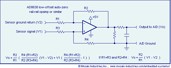
Ground loop offset errors and ground noise are eliminated by a differential amplifier or instrumentation amplifier before the analog-to-digital (A/D) conversion. The differential input amplifier addresses ground loop errors, allowing for precise measurement of non-isolated sensors. A simple operational...

This diagram represents a schematic of an RF amplifier circuit. The circuit is designed to amplify an RF signal from approximately 100 mW input power to 1.3 W output power. It utilizes a general NPN RF transistor, specifically the...
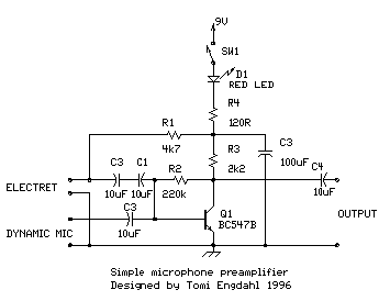
This is a simple microphone preamplifier circuit that can be used between a microphone and a stereo amplifier. This circuit is suitable for connection with standard home stereo amplifier line/CD/aux/tape inputs. The microphone preamp can accommodate both dynamic and...
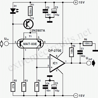
The signal from a microphone is too weak for a standard line input. This low-noise DC-coupled microphone amplifier provides a solution for anyone who wants to amplify the microphone signal effectively. A low-noise DC-coupled microphone amplifier is designed to enhance...
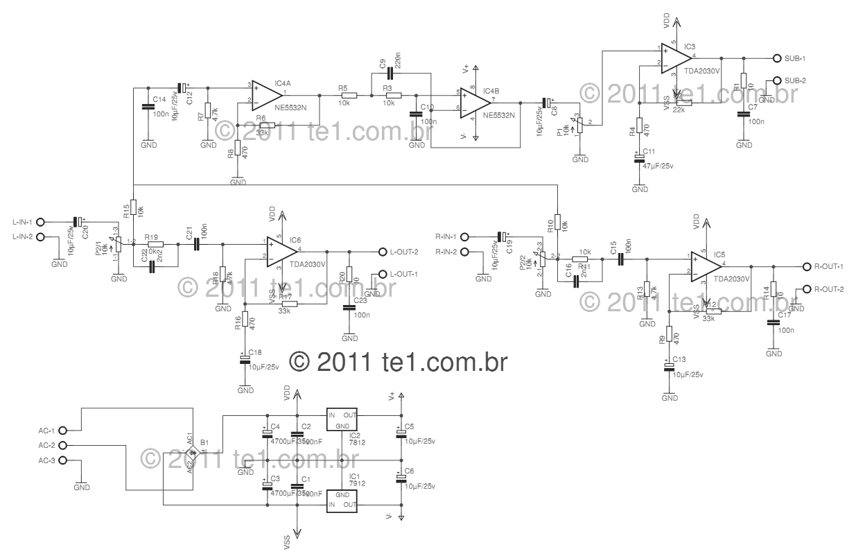
This circuit is a complete application for a 2.1 amplifier system, featuring two satellite speakers for TDA and one subwoofer. It is commonly used in commercial applications to enhance the audio output of computers using a stereo amplifier along...
Transistors are utilized as current sources, with the base drive for these transistors sourced from the main power supply VA. This configuration ensures that their collector current is proportional to the rail voltage, maintaining the voltage on the cliff-amp...