
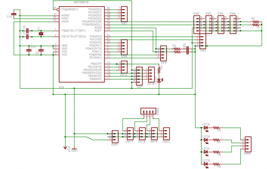
Small Breakout for SIM900 GSM Module

The UART control lines (TXD, RXD, DTR, RTS, CTS, DCD) are connected to the external area via the pin strip at contacts 12, 14, 10, 2, 4, and 6, respectively. The audio device, which includes two contacts for the microphone (with differential input) and two for the loudspeaker, utilizes contacts 15, 13, 11, and 9, corresponding to MIC1P and MIC1N (positive and negative of the microphone) and SPK1P and SPK1N (positive and negative of the loudspeaker). The RI signal, indicating incoming calls, is routed through contact 8 of the pin strip.
Transistor T1 is employed to control the cell phone's reception LED locally; its base is driven by the current logical level on pin 52 (NETLIGHT) for GSM1. The collector of this transistor connects to contact 3 of the pin strip, which is linked to the LED line, allowing the microcontroller to receive information regarding GSM network presence and the connection status of the module.
The design includes two resistors (R8, R9) for the power switch, set at 4.7k and 10k, differing from the application note's recommendation of 4.7k and 47k. This adjustment may be due to the need for reduced voltage at the base based on the choice of transistor. Additionally, a 220nF capacitor (C1) and a 10kΩ resistor (R4) are used, contrasting with the application note's configuration, which does not bridge data and VDD with a resistor and employs different capacitor values (22pF and 100nF).
The power supply design features two capacitors in parallel to ground, similar to the application note, although the suggested values differ (100µF and 0.1 to 1µF in parallel). There is interest in connecting an Arduino Mini (3.3V) to this module, with the intention of powering the device through VCC, GND, RX, TX, and RI connected to a data pin. Queries arise regarding the suitability of using the 3.3V from the Arduino Pro Mini to power the device without exceeding current limits, as the GSM module is intended for SMS functionality only. The design aims to create a custom board based on this configuration, controlled by a low-power MCU, with a preference to connect the SIM900 directly to the MCU without using pin strips.
To ensure optimal performance and reliability in the described GSM module circuit, careful consideration must be given to the power supply design, signal integrity, and the selection of components. It is crucial to maintain appropriate voltage levels and current ratings to prevent damage to the GSM module. Additionally, the layout of the PCB should minimize noise and interference, particularly in the signal paths for UART communication and audio input/output. Proper decoupling capacitors should be placed close to the power pins of the GSM module to filter out high-frequency noise. Furthermore, the use of appropriate traces and grounding techniques will enhance the overall performance of the circuit, ensuring stable operation in various conditions.The printed circuit board, has a pin strips (10 pin x 2) used to connect with the circuit board of the remote control device. The pin 1 (ON/OFF) is used by a microcontroller to turn the GSM module on and off. The module is turned on or off according to the logical level applied to their PWR line (pin 1 of GSM1).
The PWR line is equipped with an internal pull-up resistance and is active at logical zero; therefore, in order to switch the cellular module on, the microcontroller sets PWR at a high logical level (contact 1 of the pin-strip) and causes transistor T2 to saturate; this transistor will then sets the PWR line at a low level. Remember that the power on or off signal is only a pulse of about 2 seconds. Reset monitoring is handled similarly. The module can be reset by simply causing the microcontroller to send a logical 1 via the RST line, at which time the T3 transistor saturates and sets the NRESET line of GSM1 at a low level.
Let`s now proceed with UART`s control lines (i. e. , TXD, RXD, DTR, RTS, CTS, DCD), which are connected to the external area through the pin-strip`s contacts, respectively, 12, 14, 10, 2, 4 and 6. The audio device, with two contacts for the microphone (with differential input) and two more for the loudspeaker, uses contacts 15, 13, 11, 9, which correspond, respectively, to MIC1P and MIC1N (positive and negative of the microphone) and SPK1P and SPK1N (respectively, positive and negative of the loudspeaker).
The RI signal (indicating incoming calls) goes out through contact 8 of the pin-strip. Let`s now talk about transistor T1, used here to locally control the cell phone`s reception LED: its base is polarized from the current logical level on pin 52 (NETLIGHT) for GSM1. The transistor`s collector is where the line to contact 3 of the pin-strip starts; this line is connected with the LED line, which the microcontroller uses to get information regarding the presence of GSM network as well as regarding the connection status of the module (e.
g. , whether the network is available or not). Boris Landoni is the technical manager of Open-Electronics. org. Skilled in the GSM field, embraces the Open Source philosophy and its projects are available to the community. Someone has bought the other GSM breakout also in USA. Nobody said me that found problems. Thank you for the post! I have been reading the application notes on SimCom 900 and have noticed that you have put some interesting variations.
I am just curious what were the design decision, simply parts (ie: availability, commonality etc ) or if there are other considerations, I too will only use data/sms: 1). For the power switch you use two resistors (r9, r8), which you set to (4. 7k, 10k) and the application note puts them at (4. 7k, 47k). Is this simply because you need less voltage at your base due to transistor choice 3). In the same connection you use a 220nf (c1) and 10kohm resistor (r4), whereas they have a different setup (not bridging data and vdd with a resistor (r4) and they use 22pf and 100nf in their designs.
4). I notice that you use a similar design in the application note for the power supply, in that you use 2 capacitors in parallel to ground, but they suggest 100 uF and 0. 1 to 1 uF in parallel. I am looking to connect an arduino mini for now to this module (3. 3V) presumably that should work by just connecting the vcc, gnd, rx, and tx, and ri connected to a data pin or something, no Thank you for your quick response.
I meant, can I use the 3. 3v from arduino pro mini to power the device (with the board you have) Or will it draw too much current I want to use GSM Module to send SMS only. Nothing more. And i am designing my own board based on yours. It is going to be controlled by a low power MCU and i dont want to use pin strips. I just want to connect SIM900 directly to the MCU. Here is what i want to know; what should i do with the pi 🔗 External reference
Related Circuits
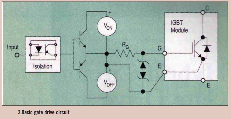
High power IGBT modules utilize hybrid integrated circuit (IC) gate drives that incorporate protection circuits, which implement desaturation detection or real-time control. High power Insulated Gate Bipolar Transistor (IGBT) modules are essential components in various high-efficiency power conversion applications, such...
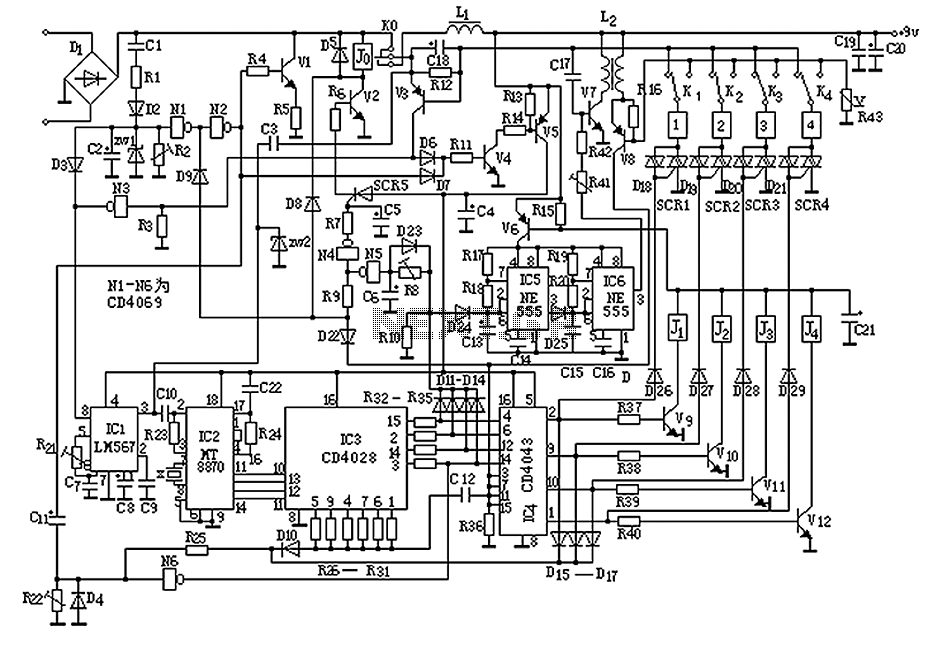
The circuit operates by sending ringing pulses through capacitor C1, resistor R1, and diode D2 to charge capacitor C2 to a voltage of 6V. This voltage causes transistors N1 and N2 to reverse, which activates V1, the analog hook,...
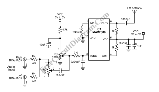
This FM transmitter circuit is compact, similar to a previous single-chip FM transmitter, but it is monophonic in nature. The circuit can be observed in the provided schematic. This monophonic FM transmitter is designed to operate on a single frequency,...
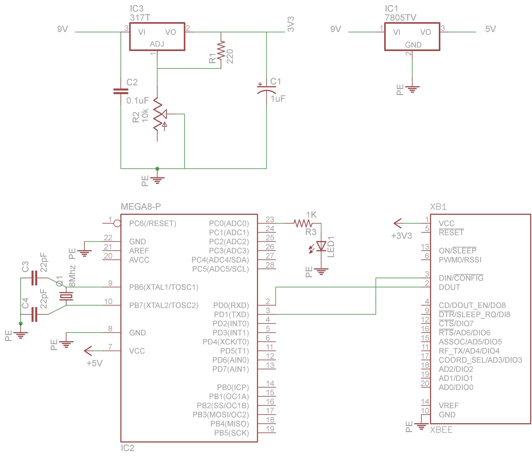
XBee modules are among the most powerful wireless communication modules available, known for their ease of configuration and use. Their cost ranges from Rs.1000 to Rs.2500, depending on the range and other specifications. It is common for users to...
This device has been designed as a demonstration application of an expandable system of modules for constructing mobile robots, adhering to the standards discussed in the Society of Robots forum. These modules can interconnect using an I2C bus, and...
After turning off TT2, the input signal enters through chi Az, where the input resistance is very high and reaches the same potential. The inverting input terminal must also be associated with this movement. Therefore, Trr functions as a...