
Small Discrete Audio Power Amplifier
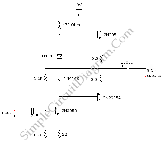
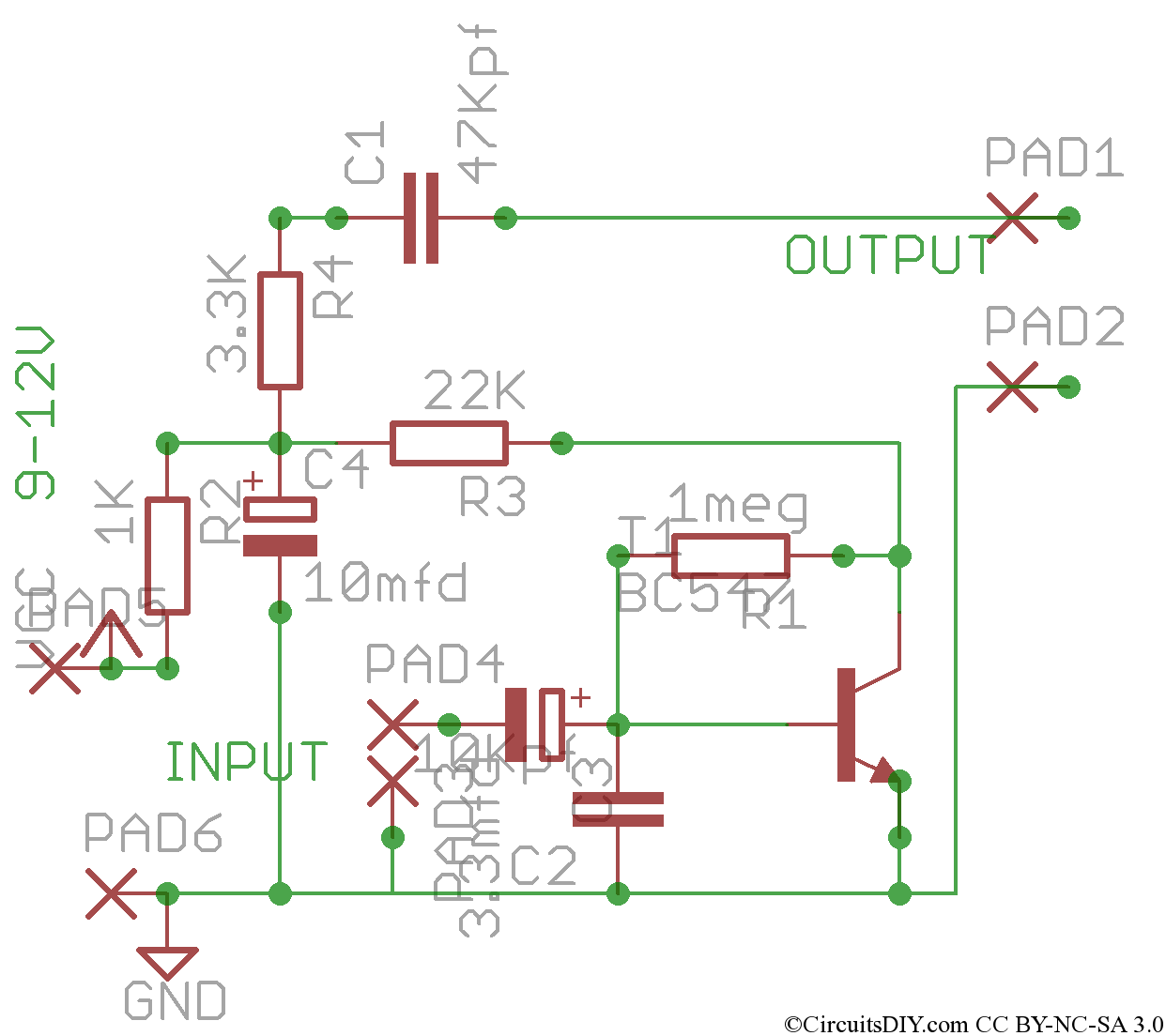
The audio amplifier circuit described utilizes a two-stage configuration, which is effective for achieving both modest power output and sound quality. The first stage, employing the 2N3053 transistor, acts as a preamplifier, receiving the audio input signal and amplifying it to a level suitable for the output stage. The output stage, consisting of a complementary pair of transistors (2N3053 and 2N2905), is designed to drive the speaker directly. This arrangement not only enhances the overall efficiency of the amplifier but also ensures that the output signal remains linear, minimizing distortion.
The biasing method employed in this circuit is crucial for maintaining consistent performance across various operating conditions. The inclusion of diodes between the bases of the output transistors serves to establish a stable operating point, compensating for variations in temperature and component characteristics. The 3.3-ohm resistor in the emitter path is a negative feedback element that helps control the gain and linearity of the amplifier, ensuring that the output remains faithful to the input signal.
The voltage gain of around 5 is adequate for driving an 8-ohm speaker, making this amplifier suitable for applications where moderate sound levels are required without the need for excessive power. The output swing of approximately 2 volts across the speaker indicates that the amplifier can deliver sufficient audio levels for personal listening devices.
For applications requiring higher power output, the use of heat sinks on the output transistors is recommended to dissipate the heat generated during operation, particularly when higher supply voltages are employed. The LM1875 integrated circuit is a viable option for those looking to build a more powerful amplifier, providing significant output capabilities while maintaining simplicity in design.
Overall, this audio amplifier circuit exemplifies an effective solution for portable audio applications, balancing performance, size, and component count while delivering satisfactory sound quality.This is a little audio amplifier, it is similar to the audio amplifier which is used in small transistor radio. This circuit draws about 30 milliamps from a 9 volt supply. This circuit consist of two stage. First stage is input stage (2N3053 transistor) and the other is output stage (2N3053 and 2N2905 transistor pair).
Here is the schematic diagra m of the circuit : Supply voltage is divided equally across the two complimentary output transistors which are slightly biased in conduction by the diodes between the bases because the input stage is biased. To stabilize the bias current so it doesn`t change much with different transistors and diodes or with temperature.
This circuit uses a 3. 3 ohm resistor that assembled in series with the emitters of the output transistors. The voltage between the base and emitter decreased, because the bias current increased, so it is reduce the conduction. This circuit has voltage gain about 5 with an 8 ohm speaker attached and input impedance about 500 ohms.
In the output stage, the voltage swing on the speaker is about 2 volts without distorting. The power output of this circuit is in the 50 milliwatt range. To provide more power we must use the addition of heat sinks to the output transistors and a higher supply voltage. With LM1875, we can build a low cost but high performance audio power amplifier. With 50V power supply, it can produce 20W output power for 4 or 8 ohm speaker. We can even get 30W output if we use 60V Continue reading †’. This audio power amplifier is very good for your portable devices, or for your headphones amplifier. The circuit of this audio power amplifier is very simple, consist of only seven components. Here is the schematic diagram of the amplifier circuit: Continue reading †’. The transistor is biased in class A. That`s mean the collector current flows all the time. This current can increase or decrease, caused by the input signal which increases and decreases the forward bias.
This increasing or decreasing depends on Continue reading †’. The basis of an audio mixer is an inverting summing circuit below. For real audio mixers, a single-supply voltage is seldom used. To increase dynamic range, the designer will often push an op amp up to, and sometimes beyond it`s Continue reading †’. We can also operate TDA8932B/33(B) from a symmetrical supply. On this diagram, three half supply voltage buffers are disabled. When supplied from a symmetrical supply, HVPREF (Pin 11), HVP1 (pin 30) and HVP2 (Pin 19) should be connected to ground.
Continue reading †’. 🔗 External reference
Related Circuits
Section Ul-a is configured as a high-gain inverting voltage amplifier that is inductively coupled to the phone line via LI. Inductor LI is a homemade unit that consists of 250 turns of fine, enamel-coated wire that is wound on...
The output of this circuit should be connected to a high-impedance load, typically greater than 100K ohms, while noting that the impedance of capacitor C4 is approximately 3K ohms. A PNP transistor may also be utilized, requiring adjustments to...
.gif)
This circuit utilizes a single integrated circuit (IC) along with a minimal number of external components to display audio levels through ten LEDs. The input voltage range is from 12V to 20V, with a recommendation for 12V. The LM3915...
The amplifier circuit presented in this paper introduces a floating power supply aimed at increasing output power. The output power of the amplifier is influenced primarily by the final stage amplifier supply voltage. The circuit's principle is illustrated in...
This circuit consists of a single transistor functioning as an amplifier, providing significant amplification for weak and unipolar signals, which can then be fed into a more powerful amplifier. The described circuit utilizes a single transistor in a common-emitter...
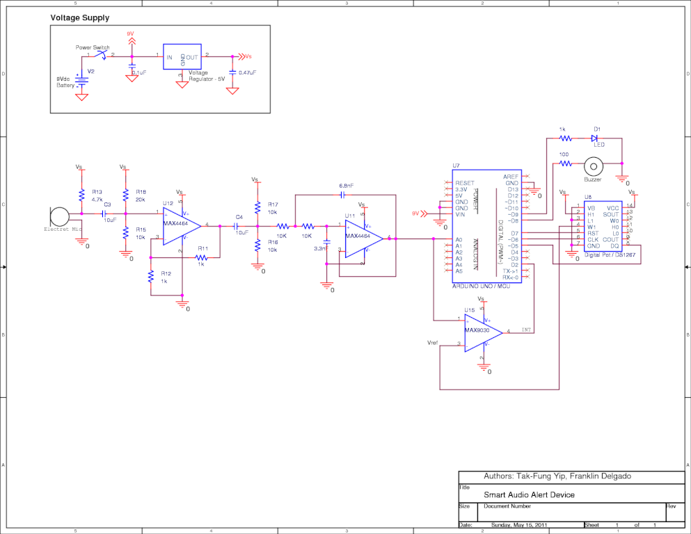
This is a senior project from Stony Brook University, designed and implemented by Tak-Fung Yip and Franklin Delgado, with consultation from Professor Milutin Stanac. The senior project from Stony Brook University represents a collaborative effort in the field of electronics...