
Soft Musical Telephone Ringer by UM66T
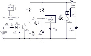
The circuit operates as a ringing detector and audio signal generator, utilizing a combination of transistors, resistors, capacitors, and a diode. Transistor T1 serves as the primary detection element for the incoming ringing voltage, while T2 acts as a switch that controls the state of the audio output. Resistor R2 plays a crucial role in biasing T2, ensuring it remains in a conducting state when no ringing voltage is present.
Capacitor C2 is essential for maintaining the circuit's functionality during the ringing intervals. It temporarily stores charge, allowing for rapid discharging through T1 when the ringing voltage is detected. The forward biasing of T1 by the ringing voltage leads to a quick discharge of C2, which effectively transitions T2 to the off state, enabling IC1 to produce an audio output.
Diode D1 ensures that the forward biasing of T1 occurs only during the positive half of the ringing cycle, providing a unidirectional path for the current and protecting the circuit from reverse voltage conditions. The output from IC1 is then fed to the base of transistor T3, which amplifies the audio signal to drive a speaker, producing sound.
This configuration allows the circuit to respond dynamically to the incoming ringing signal, generating an audio output only when a valid ringing voltage is detected. During the negative half of the ringing cycle, the inability of capacitor C2 to charge quickly through R2 ensures that the circuit remains inactive, preventing unwanted audio signals from being generated. The design effectively combines detection and audio generation, making it suitable for applications such as telephone ring signal indicators or alert systems.The incoming ring is detected by transistor T1 and components wired around it. In absence of ringing voltage, transistor T1 is cut off while transistor T2 is forward biased as resistor R2 is returned to the positive supply rails. As a result collector of transistor T2 is at near-ground potential and hence IC1 (UM66) is off. Also capacitor C2 is ch arged to a slightly positive potential. During positive half of the ringing voltage, diode D1 forward biases transistor T1 and rapidly discharges capacitor C2 to near ground potential and cuts off transistor T2 which, in turn, causes IC1 to be forward biased and music signal is applied to base of transistor T3 which drives the speaker. During negative half of the ringing voltage, capacitor C2 cannot charge rapidly via resistor R2 and hence transistor T2 remains cut off during the ringing interval.
🔗 External reference
Related Circuits
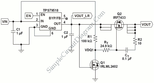
A PMOS FET switch regulator output is utilized in series with the regulator's load, as illustrated in the accompanying diagram. This represents a straightforward approach to circuit design. The described configuration employs a PMOS FET as a switching element in...
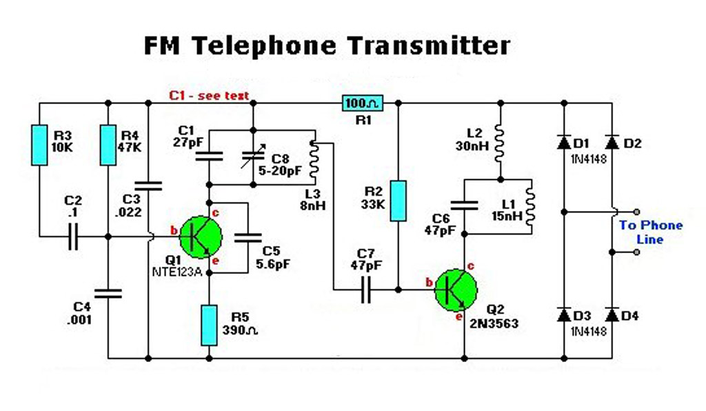
Electronic FM Telephone Transmitter Schematic. The following schematic design illustrates a circuit diagram for an FM telephone transmitter built on a compact PC board layout. This small design allows it to be easily integrated within the housing of a...
The circuit is designed to connect in parallel with a telephone, displaying the dialed number using DTMF (Dual Tone Multi-Frequency) signaling. It can also show the number dialed from the receiving party's phone, making it useful for capturing numbers...
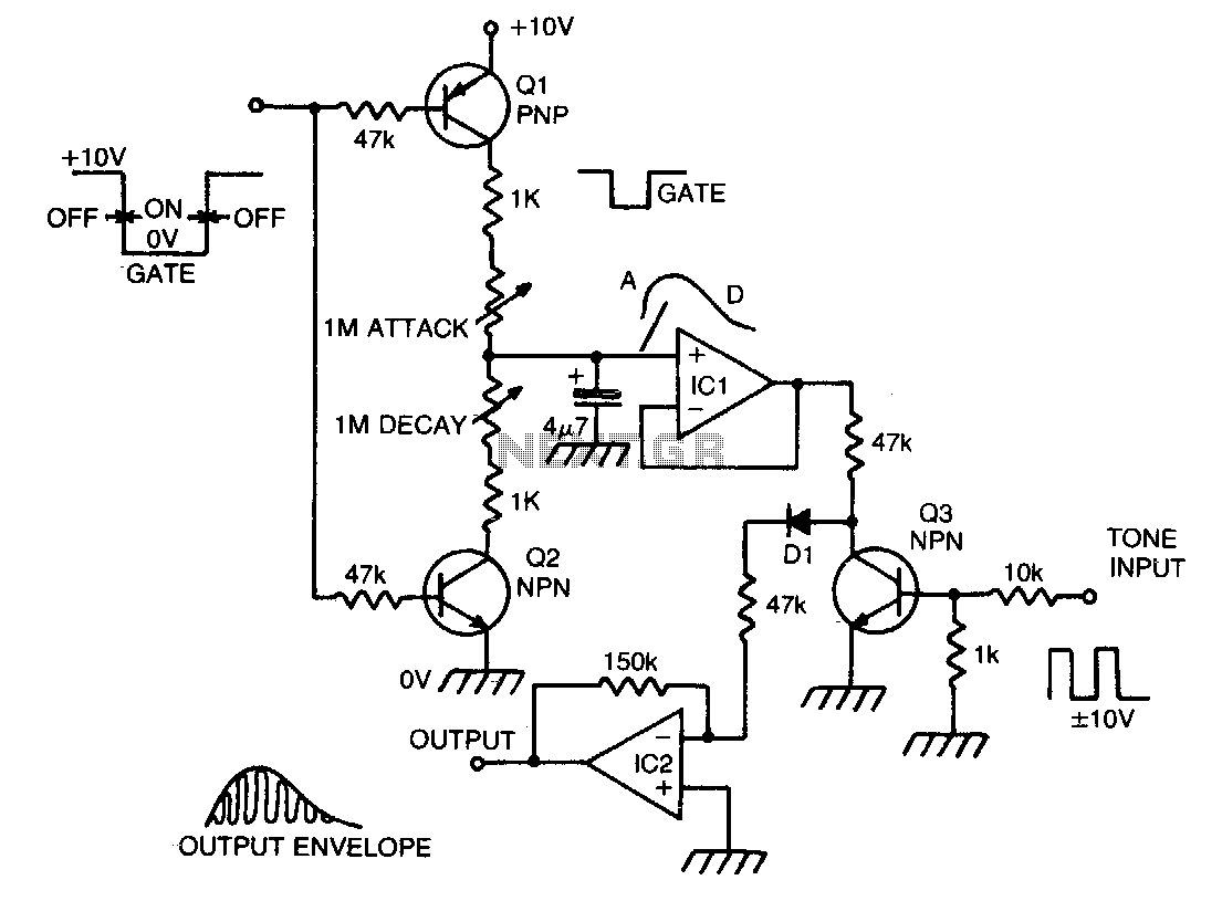
When a gate voltage is applied, Q1 is activated, and capacitor C is charged through the attack potentiometer in series with a 1 KΩ resistor, which varies the attack time constant. A fast attack results in a percussive sound,...
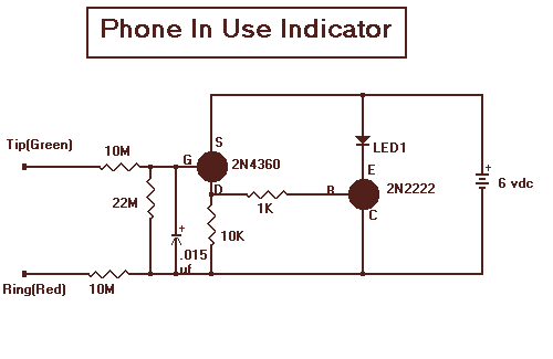
With this circuit mounted in or near every phone in the house, it will allow users to know if the phone is being used and not to pick up the phone. When a phone is taken off hook, the...
This circuit generates a ringing sound akin to that produced by modern telephones. It comprises three nearly identical oscillators arranged in a sequence, each responsible for generating a square wave signal. The frequency of each oscillator is determined by...