
SPDIF Monitor Circuit
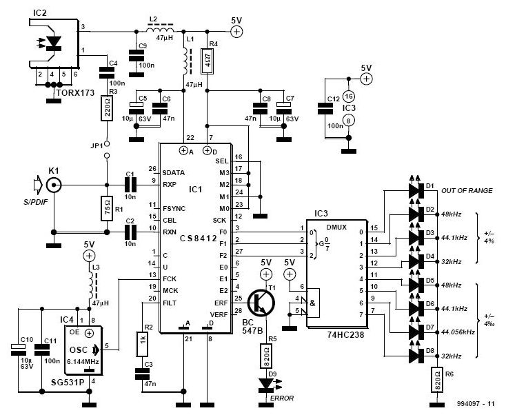
The S/PDIF monitor circuit utilizes the CS8412 receiver to facilitate the reception and decoding of digital audio signals. The CS8412 is a versatile component that supports various digital audio formats, making it suitable for applications in audio processing and monitoring. The inclusion of an external reference oscillator (IC4) enhances the circuit's ability to accurately compare incoming signal frequencies against a stable reference, thereby improving the overall performance of the monitor.
The optical input provided by IC2 is a critical feature that allows for the reception of digital audio signals via optical fiber, a common method for transmitting high-quality audio. The output configuration involving R1, C4, R3, and jumper JP1 is designed to allow flexibility in how the output voltage is utilized, which can be essential for interfacing with different types of digital systems.
The circuit's ability to function as a relay station or jitter reducer is particularly valuable in professional audio applications, where signal integrity is paramount. By configuring IC1 in mode 13, the circuit can bypass certain processing steps, allowing for a more direct transfer of the S/PDIF data to the output. This configuration ensures that the bit clock operates at an optimal frequency, which is crucial for maintaining synchronization in digital audio systems.
The addition of a demultiplexer (IC3) to decode the audio data into individual channels for visual indication via light-emitting diodes provides a user-friendly interface for monitoring signal quality. The presence of diode D9 serves as a diagnostic tool, alerting users to potential issues with signal reception. Overall, the S/PDIF monitor circuit is a sophisticated solution for monitoring and processing digital audio signals, with various applications in both consumer and professional audio environments.The SPDIF monitor is one of the many applications possible with the digital audio interface receiver Type CS8412 from Crystal. Other applications described in earlier issues of this magazine dealt with the decoding of the S/PDIF (Sony/Philips Digital Interface Format) into data, bit clock and L/R clock in a digital voltmeter or clipping indicator.
The addition of an external reference oscillator, IC4, enables the receiver to differentiate incoming signals by means of a frequency comparator and this is what the present monitor does. When the frequency of an incoming signal differs from a reference value, the difference is indicated in one of three ways: Clearly, the accuracy of the crystal oscillator determines the precision of these limits (the SG531P crystal from Epson used in the diagram has an accuracy of ±100 ppm).
The optical input provided by IC2 is a useful addition. The output of this circuit is applied across R1 via C4, R3 and jumperJP1. The potential across R1 may also be used as a digital output, in which case the value of R3 needs to be adapted as necessary. The circuit may also be used as a kind of relay station or as a means for reducing jitter. For these purposes, IC1 is connected in a special mode (mode 13) when M3 is made 1, and M0 M2, 1, 0, and 1, respectively.
When these levels are set the received S/PDIF data, including the preamble, is transferred directly to the output. The bit clock, SCK, then has a value twice as high as would be the case with coded data. It is possible to connect a TOSLINK module, or a coaxial output via a buffer (such as a number of parallel-linked 74HC04 inverters), to the SDATA output.
A demultiplexer, that is, 3-to-8 line decoder IC3, is used to decode the data at F0 F2 to eight separate light-emitting diodes. Diode D9 indicates whether IC1 receives no or poor data. The overall circuit draws a current of not more than 35 mA. 🔗 External reference
Related Circuits
This compact circuit enables automatic recording of phone conversations. It connects to the phone line, the microphone input of a tape recorder, and the remote control jack of the recorder. The circuit detects the voltage level in the phone...
All of the components in this list are generally available through RadioShack for less than $20. It is highly recommended to use a breadboard for assembly, as mistakes are common for first-time builders, and soldering can complicate troubleshooting. This...
As shown in the figure, the 555 timer, resistors R1, RP1, and capacitor C1 form a controlled audio oscillator. The frequency of the oscillator is given by the formula f = 1.44 / ((R1 + 2 * RP1) *...

This simple circuit can be used to flash incandescent lamps with a power rating of up to 10W. It is ideal for creating flashing beacons on automobiles and similar applications. The circuit consists of an astable multivibrator utilizing transistors...
The Quick and Easy Wireless circuit is not overly complex, but it requires careful verification of connections before initial operation. Key components in the circuit include the 7805 voltage regulator, the 18F452 microcontroller, an RC Receiver, and an RC...
The K8000 DAC High Power Amplifier is an electronic amplifier with an adjustable output voltage ranging from 0 to 9 V and capable of delivering an output current of up to 9 Amperes. The K8000 DAC High Power Amplifier is...