
Split Phase-Data Synchronizer and Decoder

The timing diagram of Waveform A provides a visual representation of the split-phase data signaling method, which is commonly used in digital communication systems. In this format, data is transmitted in two distinct phases, allowing for improved synchronization and error detection. The binary digits, or bits, are represented as high and low voltage levels, corresponding to logical '1' and '0', respectively.
Each bit in the waveform has a defined duration, which is crucial for ensuring that the receiving end can accurately interpret the signal. The periodic nature of the signal is characterized by a consistent time interval between the transitions of each bit, which is essential for maintaining the integrity of the data transmission.
In a practical application, the split-phase data signal can be utilized in various communication protocols, such as UART (Universal Asynchronous Receiver-Transmitter) or SPI (Serial Peripheral Interface). The timing diagram aids in understanding the timing relationships between the bits, including rise and fall times, as well as the setup and hold times required for reliable data sampling.
The waveform's characteristics can be further analyzed to determine parameters such as the frequency of the signal, the duty cycle, and potential signal integrity issues that may arise due to noise or distortion. Overall, the timing diagram serves as a fundamental tool for engineers to design, troubleshoot, and optimize digital communication systems.Waveform A is timing diagram that shows A split-phase data signal. It consist of a series of binary digits that occur at a periodic rate. Duration of each bit.. 🔗 External reference
Related Circuits
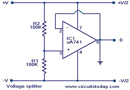
Voltage splitter using op-amp uA741 IC, circuit diagram, working, description. The voltage splitter circuit utilizing the uA741 operational amplifier (op-amp) is designed to provide a stable output voltage that is a fraction of the input voltage. The uA741 is a...
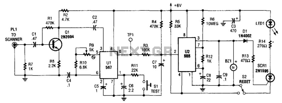
This circuit detects the 1050-Hz tone transmitted by NOAA (National Oceanic and Atmospheric Administration) weather radio stations, which operate within the frequency range of 162.40 to 162.55 MHz. The tone is emitted for several seconds. Q1 functions as an...
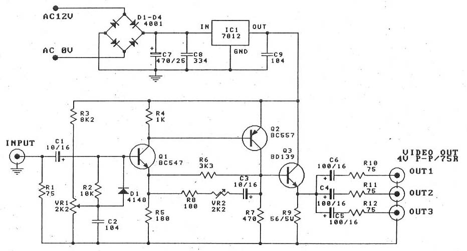
This is a video amplifier circuit or video splitter circuit, designed to strengthen video signals. It compensates for signal loss and is... The video amplifier circuit serves as a crucial component in video signal distribution systems, ensuring that the integrity...
The MT8870 is a complete DTMF receiver that integrates both the band-split filter and digital decoder functions. The filter section employs switched capacitor techniques for high and low group filters, while the decoder utilizes digital counting methods to detect...
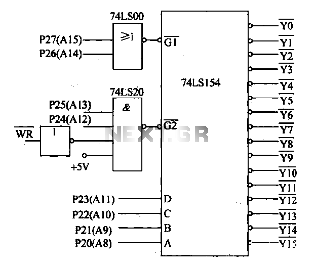
Decoding circuit: To ensure proper functionality of various interfaces, the system must assign IP addresses to all ports. Based on the number of system interfaces, it utilizes the 74LS154 decoder, which can translate up to 16 addresses. The interface...
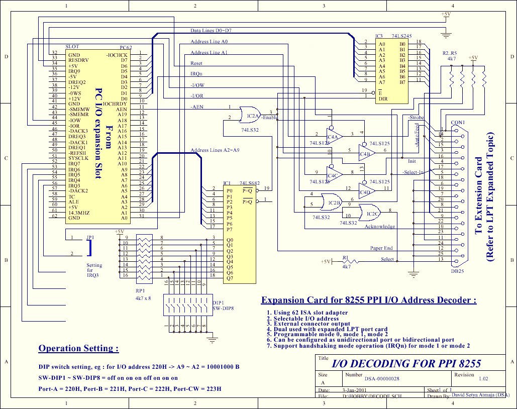
The PPI-8255 is a general-purpose I/O programmable interface that is typically connected directly to a computer bus. This article demonstrates that the card can serve dual purposes: as an expander port and for direct I/O functionality. The card can...