
Static Electricity / Negative Ion Detectors
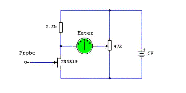
The described circuit emphasizes the importance of sensitivity in the gate terminal, which is crucial for applications involving electric field detection. The open-circuit configuration allows for high sensitivity to voltage fluctuations, making it suitable for detecting weak signals or environmental changes. The use of a bare copper wire as a probe enhances the circuit's responsiveness, as it minimizes additional capacitance or inductance that could affect performance.
The choice of not using veroboard or PCB materials is particularly relevant, as these materials can introduce parasitic capacitance that would lower the gate impedance and compromise the circuit's sensitivity. An open construction technique is recommended to maintain the integrity of the circuit's performance. Soldering each component in a center zero configuration ensures that connections are secure while minimizing interference.
The full-scale deflection specifications of 1mA or 250µA indicate that the circuit can be calibrated for different sensitivity levels, depending on the application requirements. The adjustment of the preset resistor to achieve a zero voltage reading between the FET drain and the preset resistor is a critical calibration step. This ensures that the circuit accurately reflects the changes in voltage without any offsets that could lead to erroneous readings.
Monitoring the circuit's response by moving the probe in front of the detector allows for real-time assessment of its functionality. This dynamic interaction can reveal how effectively the circuit responds to varying electric fields, providing valuable insights into its operational capabilities. The ability to visualize the effects of charge changes enhances the practical understanding of the circuit, making it a valuable tool for applications in fields such as sensing, detection, and research in electromagnetic phenomena.the gate terminals sensitivity to changes in voltage. The gate terminal here is left open circuit, connected only to the "probe" this being just a few inches of bare copper wire. With no fixed DC biasing, the gate terminal will respond to micro changes in voltage or "field strength".
It is important not to make this circuit on veroboard or PCB mat erial as this will reduce the effective gate impedance. Instead use an "open" construction technique soldering each component should be a centre zero type. Full scale deflection can be 1mA or 250uA for greater sensitivity. Remove the meter and use a multimeter to measure the voltage between FET drain and the preset resistor. Adjust the preset for 0 volts and then replace the meter. This will avoid can be monitored by moving the probe in front of it. As the detector responds to changes in charge, you may need to move the detector around to see the effect, but it will prove the
🔗 External reference
Related Circuits
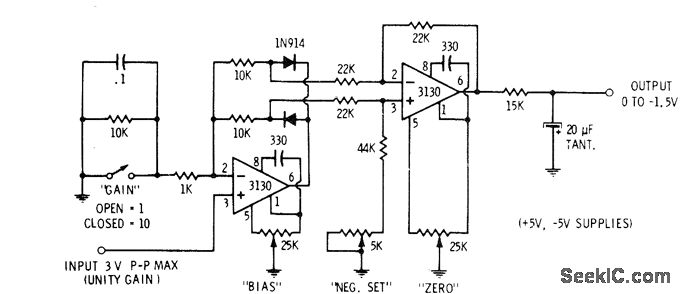
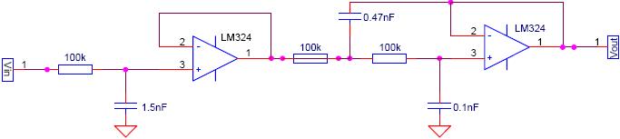
This circuit is utilized in digital voltmeters to convert an AC waveform into a full-wave rectified DC equivalent. The first operational amplifier (op-amp), designated as 3130, functions as a polarity separator. Negative-going signals appear across the upper 10K resistor,...
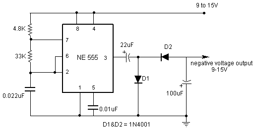
Opamps are very useful. But one of their major drawbacks is the requirement of a dual supply. This seriously limits their applications in fields where a dual supply is not affordable or not practicable. This circuit solves the problem...
DBS-20 type leakage protection circuit The DBS-20 type leakage protection circuit is designed to detect and prevent electrical leakage, thereby enhancing safety in electrical installations. This circuit operates by monitoring the current flowing through the live and neutral conductors. When...
The HCS12 series of microcontrollers does not include dedicated internal digital-to-analog conversion hardware. Therefore, external hardware, such as a digital-to-analog conversion integrated circuit (IC), is required. To implement digital-to-analog conversion (DAC) in systems utilizing the HCS12 microcontroller, an external DAC...
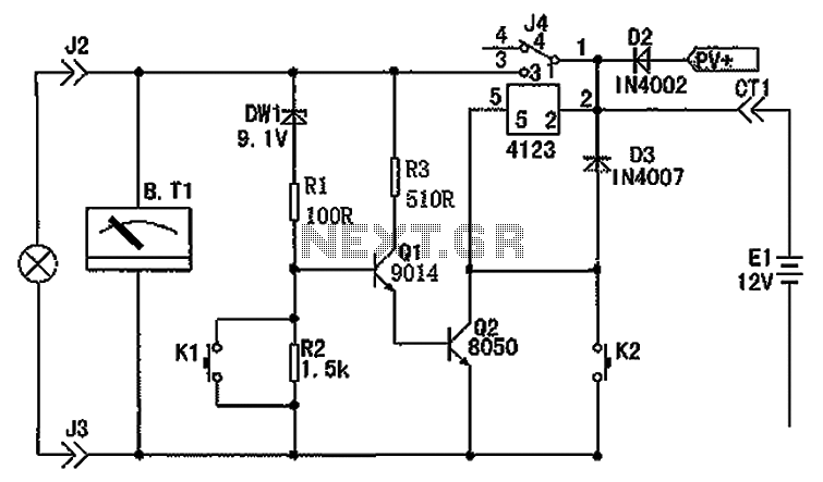
The circuit depicted in the figure consists of a battery, a controller, and various electrical and charging components. It includes a Zener diode (D1) and resistors (R1, R2) for undervoltage detection. The circuit also features transistors (Q1, Q2), resistors...
TCA440 is an AM receiver circuit designed for long wave (LW), medium wave (MW), and short wave (SW) applications in both battery-operated and line-operated radio receivers. It features an RF pre-stage with automatic gain control (AGC), a balanced mixer,...