
step down switching converter
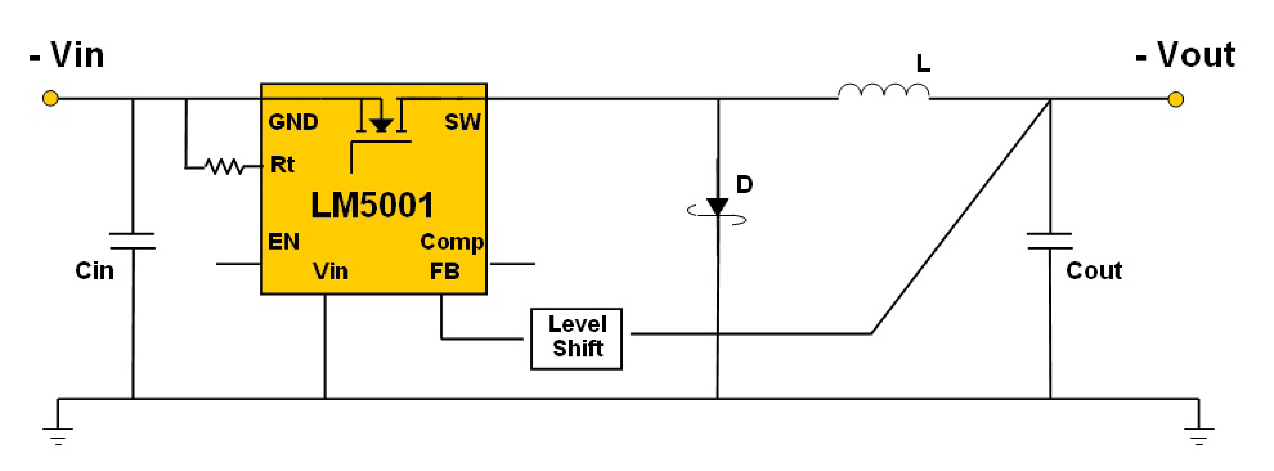
The negative buck topology is a specialized configuration that allows for the conversion of negative input voltages to negative output voltages while maintaining a common ground. This topology is particularly useful in applications where negative voltage supplies are required, such as in powering operational amplifiers or certain types of sensors. The architecture typically consists of a high-side NFET, an inductor, a catch diode, and an output capacitor.
The high-side NFET is essential for controlling the flow of current from the input to the output. When the NFET is turned on, current flows through the inductor, storing energy in its magnetic field. When the NFET is turned off, the energy stored in the inductor is released to the output through the catch diode, which prevents reverse current flow. The LC output filter smooths the voltage at the output, providing a stable negative voltage.
In terms of control, the feedback loop in a negative buck regulator is critical for maintaining the desired output voltage. The feedback circuitry typically involves a voltage divider that senses the output voltage and feeds it back to the control IC. The control IC adjusts the duty cycle of the PWM signal driving the NFET based on the feedback to regulate the output voltage effectively.
When selecting components for a negative buck converter, several factors must be considered, including the maximum output current, input voltage range, and thermal management. The choice of the NFET is particularly important, as it must be able to handle the maximum switch current and have a low Rdson to minimize power losses. Additionally, the layout of the PCB should be optimized to reduce parasitic inductance and capacitance, which can affect the performance of the converter.
In summary, negative buck converters are a valuable tool in power electronics, providing a means to generate negative voltages from negative inputs. Understanding the unique requirements and characteristics of this topology is essential for successful implementation in various applications.High-efficiency step-down switching regulators for positive voltages are very common, however negative step-down switching regulators (negative voltage in, negative voltage out, common ground) are not as well known, even though they are often needed. Although they are not difficult to set up, literature on how to build them is rather scarce. Thisarticle analyzes the architecture and detailed operation of the negative buck topology. It will also discuss actual circuit implementations for the topology, from a system perspective down to the building of the needed circuit blocks, and include examples on how to build a voltage translator circuit, a key block in implementing a negative buck regulator using readily available boost ICs. (Note: In the figure, while it is common to draw positive rails at the bottom of circuits in schematic diagrams and, based on it, negative buck topologies show ground (most positive rail) on the top in many cases.
Here, ground was drawn at the bottom with the circuit`s Vin and Vout at the top on purpose, to reflect the simplicity and similarity of this topology compare to the positive buck. ) Like a positive buck design, it has a high-side pass device between input and output, an LC output filter, and a catch diode.
The two big differences are the gate drive needed in the control IC and the feedback circuitry. In a positive buck, a typical NFET used as a high-side pass device requires a gate-drive voltage higher (more positive) than the systems input voltage (Vin) in order to be turned on. Since the input voltage is the most positive voltage in the system already, special circuitry is needed to generate an even higher voltage.
Positive buck ICs have usually this function built in. In a negative buck, an NFET used as a high-side pass device also requires a gate-drive voltage more positive than the system`s input (-Vin). In this case, since this input voltage is the most negative voltage in the system, though no special circuitry is needed.
All other voltages, including the output, are "higher" (more positive), with the converter ground being the most positive voltage in the system. Under these circumstances, a low-side FET PWM control IC (such as a boost/flyback regulator or controller) can be used to implement the converter.
A variety of ICs may be used to implement negative buck converters, including controllers and integrated monolithic regulators with low side NFETs. Monolithic ICs provide simplicity, ease of implementation and lower component count. Controllers offer greater flexibility, particularly when larger output currents are needed, as well as when there`s the need to optimize for efficiency and thermal dissipation, than can be achieved by choosing a FET with optimal Rdson, packaging, turn-on and turn-off times, and other factors for the requirements.
It is a 3. 1 to 75 volt input-voltage-range device from National Semiconductor that has a built-in 75 V, 1 A NFET. In a regular boost application, the LM5001 will put out a gate-drive voltage to its built-in pass NMOSFET a few volts above ground in order to turn it on.
In a negative buck application, the gate drive will still put out a gate voltage a few volts above the IC`s ground pin, which in this case is tied to the system`s input voltage (-Vin) and will yield the results needed. Different from a regular boost, but the same as a regular buck, peak IC-switch current in Figure 2 is the same as peak inductor/output current, thus allowing a 1 A boost IC to be used for output currents up to 1 A.
Other regulators with different ratings would be used for higher or lower switch currents. If a controller is preferred, it would be used in a similar configuration to the one in the figure. The other special consideration in a negative buck architecture using an off-the-shelf boost IC is the signal conditioning needed for the feedback path. Most ICs require a voltage around 1. 25 V (relati 🔗 External reference
Related Circuits
This power supply employs two VN400A 400-Volt MOSFETs arranged in a half-bridge configuration. The outputs provide +5V at 20A and +15V at 1A. Low-current outputs utilize three-terminal regulators, allowing for either 12 Volts or 15 Volts to be achieved...
A DC/DC step-up converter is suitable for use in battery-powered equipment. This converter can be employed to generate supply voltages for internal circuits. The DC/DC step-up converter, also known as a boost converter, is a critical component in various electronic...
This power supply utilizes an SGS-Thomson UC3842 integrated circuit in an off-line flyback regulator configuration, delivering +5 V at 4 A and ±12 V at 300 mA. This design allows for the use of a compact high-frequency (50 kHz)...
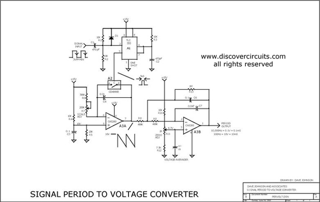
This circuit is designed to convert a square wave input signal into a voltage output. The voltage produced is proportional to the time interval between the edges (period) of the signal, rather than its frequency. The operational range of...
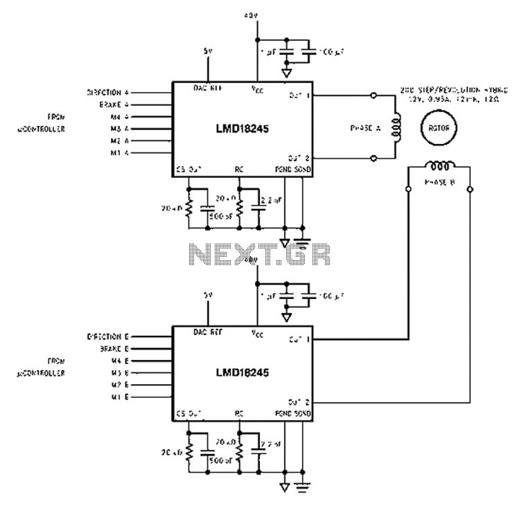
An innovative current detection method eliminates the power loss associated with the sense resistor in series with the motor. A 4-digit analog converter (DAC) facilitates digital control of the motor current path, simplifying the implementation of full, half, and...
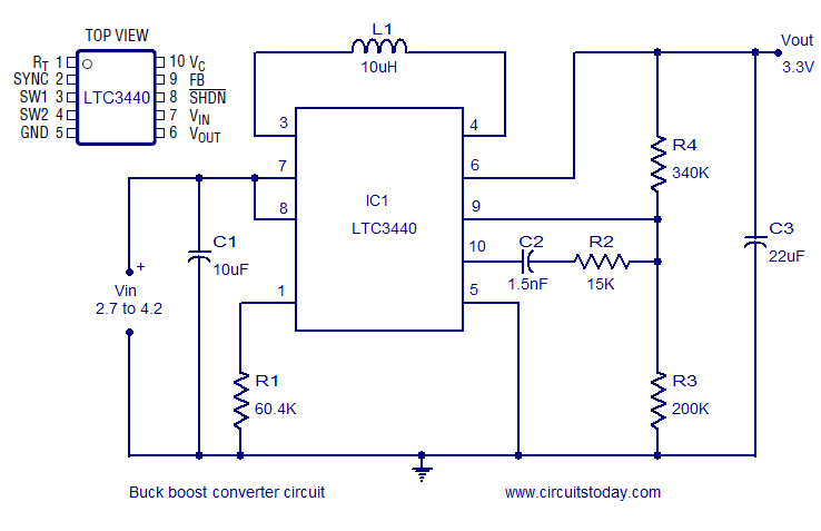
A simple and highly efficient buck-boost converter is implemented using the LTC3440 integrated circuit. The output voltage is set at 3.3V, while the input voltage range can vary from 2.7V to 4.2V. The LTC3440 is a synchronous buck-boost converter designed...