
Switch Debouncer With Auto Repeat

This circuit can be analyzed in terms of its key components and their interactions. The pushbutton switch SW1 acts as the input trigger, initiating the pulse generation when pressed. The hysteresis gate oscillator, utilizing a 74HCT14 Schmitt trigger, provides a stable output by ensuring that the output state changes only when the input crosses specific voltage thresholds.
Diode D1 serves to create asymmetry in the charge and discharge cycles of capacitor C1, which is critical for defining the timing characteristics of the oscillator. The resistor R2 plays a role in controlling the discharge path of C1, thereby influencing the time it takes for the capacitor to reach the upper gate threshold of 2.3 V.
The DBRT is a crucial parameter that defines the delay before the oscillator can repeat its cycle. It is determined by the time required for C1 to charge to the upper threshold, which is a function of the circuit's resistive and capacitive components. The hysteresis effect, characterized by a voltage difference of less than 1 V, ensures that noise does not cause false triggering of the output pulse.
The relationships between the resistors R1, R2, and R3 are significant in ensuring that R1 is much smaller than R3, and R2 is much smaller than R1. This configuration allows for optimal performance of the oscillator, ensuring that the timing and pulse generation are reliable and consistent. The circuit design is thus a balance of component values that achieves the desired output characteristics while maintaining stability and responsiveness in pulse generation. This circuit produces an output pulse when SW1 (pushbutton) is depressed. It also becomes a hysteresis ga te oscillator. Dl and R2 add asymmetry. The DBRT (delay before repeat time) is caused by the oscillator start-up conditions: CI has to change from zero to the upper gate threshold rather than to the lower threshold. The auto repeat time: Gate hysteresis « 1 V for 74HCT14 gate, DBRT= 0.7T (upper gate threshold hysteresis).
Upper gate threshold 2.3 V for HCT14, Ri<
Related Circuits
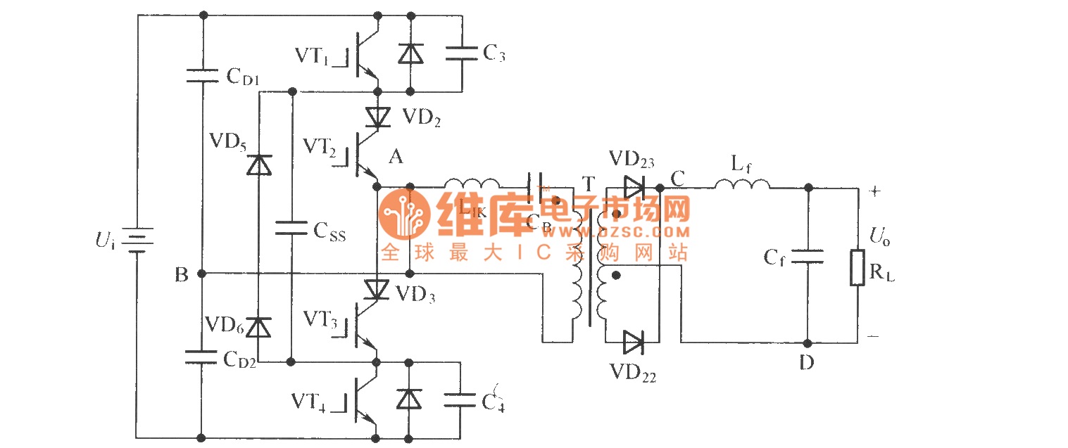
To eliminate circulating current in a zero-voltage switch three-level DC converter during its zero state, a zero-voltage zero-current switch three-level DC converter circuit has been proposed. The primary distinction between this circuit and the standard zero-voltage switch three-level DC...
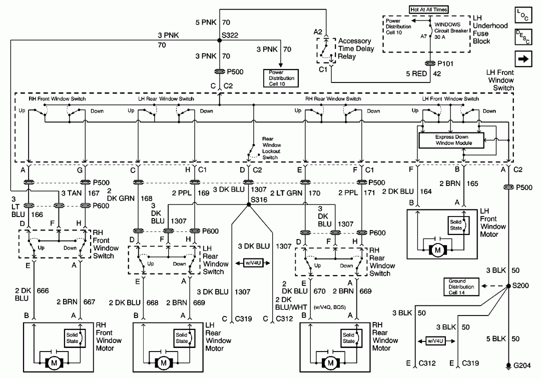
The system utilizes a single circuit breaker instead of fuses. According to the schematic, switches provide 12 volts of power and ground to the window motors in opposite polarities, allowing the windows to move up and down. Troubleshooting should...
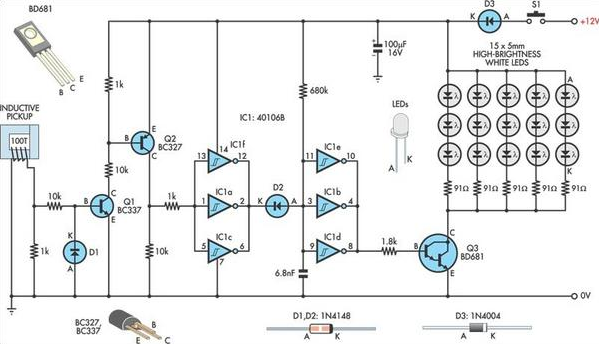
A useful timing strobe can be constructed using high-brightness LEDs and a few common components. Ignition pulses from the number 1 cylinder high-tension lead are used to trigger the circuit via a homemade inductive pickup. Transistors Q1 and Q2...

This circuit employs a flip-flop configuration utilizing Q1 and Q2. Under normal conditions, Q1 is heavily conducting. When light is detected by the CDS photocell, the bias on Q1 decreases, resulting in its cutoff, which activates Q2 and removes...

This signal tracker and lock detector combine to create a precision tone switch. The filter composed of R3, R4, and C2 determines the signal capture and tracking range, as well as the settling time. The maximum VCO frequency is...
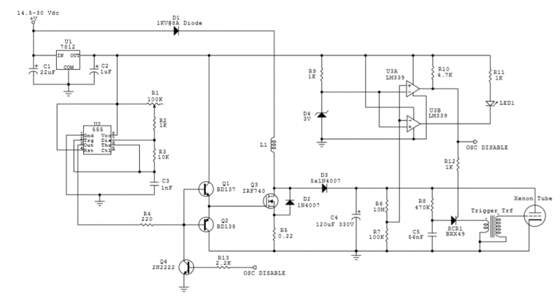
The circuit utilizes an IRF740 MOSFET, which has a maximum drain-source voltage (V_DS) rating of 400V. The avalanche voltage is calculated to be approximately 3520V, indicating that up to about 500V of inductive kickback voltage can develop in the...