
Automotive LED Timing Light
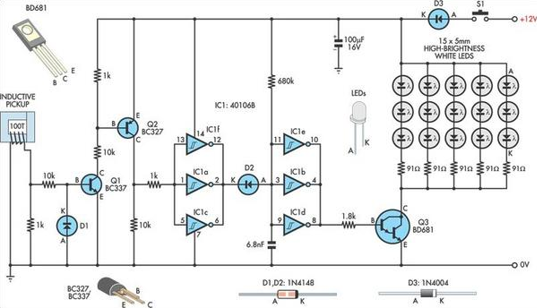
This timing strobe circuit utilizes high-brightness LEDs as the primary visual output, activated by ignition pulses from the number 1 cylinder of an engine. The circuit is initiated using a homemade inductive pickup, which detects the high-tension lead's electromagnetic field. The output from the pickup is first buffered and amplified by transistors Q1 and Q2. This amplification ensures that the subsequent signals are strong enough to drive the inputs of the Schmitt-trigger inverters, specifically IC1a, IC1c, and IC1f.
The Schmitt-trigger inverters are critical for converting the pulsed input signals into a clean output. Each inverter generates a low output pulse in response to a positive input pulse, which forward-biases diode D2. This action discharges the 6.8nF capacitor immediately. As the capacitor discharges, it creates a logic low condition at the inputs of the second set of inverters (IC1b, IC1d, and IC1e). Consequently, these inverters output a high signal, which activates transistor Q3, thereby powering the LED array.
The timing of the LED illumination is controlled by the capacitor's charge and discharge cycle. After the initial pulse from the ignition, the outputs of IC1a, IC1c, and IC1f return to a high state, reverse-biasing D2. The capacitor's charging time to reach the logic high threshold of the inverters effectively lengthens the duration of the LED illumination, providing a strobe effect that can be adjusted based on the capacitor's characteristics.
For the inductive pickup, it is recommended to use a C-type ferrite or powered iron core, which should be wrapped with approximately 100 turns of light-gauge wire to ensure effective signal capture. The design may require some adjustments to the number of turns based on experimental results to achieve optimal triggering performance. To maintain signal integrity and minimize interference, a miniature screened microphone cable is advisable for connecting the pickup to the circuit. This setup provides a robust and effective method for visual timing indications in automotive applications.A useful timing strobe can be constructed using high-brightness LEDs and a few common components. Ignition pulses from the number 1 cylinder high-tension lead are used to trigger the circuit via a home-made inductive pickup. Transistors Q1 & Q2 buffer and amplify the pulses from the pickup, which then drive the inputs of three Schmitt-trigger inve
rters (IC1a, IC1c & IC1f). Each positive pulse at the inverter inputs causes a low pulse at their outputs, forward-biasing D2 and immediately discharging the 6. 8nF capacitor. When the capacitor is discharged, the inputs of the second bank of three inverters (IC1b, IC1d & IC1e) see a logic low level, so their outputs go high, driving Q3 into conduction and powering the LED array.
After the pulse ends, the IC1a, IC1c & IC1f inverter outputs return high, reverse biasing D2. However, it takes some time for the 6. 8nF capacitor to charge to the logic high threshold voltage of the inverters` inputs, effectively stretching the initial pulse width and lighting the LEDs for the required amount of time. The pickup can be salvaged from an old Xenon timing light or made up from a C type ferrite or powered iron core large enough to fit around a HT lead.
Some experimentation will be required to determine the number of turns required to achieve reliable triggering. About 100 turns of light-gauge wire proved sufficient on the prototype. A cleat is used to close the magnetic path around the lead and is held in place with a large battery clip.
Miniature screened microphone cable can be used to connect the pickup to the circuit, to prevent interference from other sources. 🔗 External reference
Related Circuits
Decorative lights arranged in various moving patterns are visually appealing and have gained significant popularity in today's world. While more complex lighting arrangements may require the use of microcontroller ICs, simpler yet captivating light effects can be generated using...

A clock-controlled relay, also known as a time delay relay, allows for the automatic activation of a load, such as a water pump, at a predetermined time. This device utilizes a standard clock mechanism to trigger the circuit, enabling...
When sufficient light reaches the Light Dependent Resistor (LDR) in this circuit, an alarm tone is activated on the loudspeaker. This tutorial guides beginners in electronics through the step-by-step process of constructing the circuit on a breadboard. The circuit utilizes...
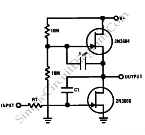
This is a JFET AC Coupled Integrator circuit. This circuit is used to achieve very high voltage gain. To achieve very high voltage gain, this circuit uses... The JFET AC Coupled Integrator circuit is designed to provide significant voltage amplification...

The brightness of an LED display is adjusted by utilizing a photocell in place of one timing resistor in a 555 timer configuration, while bypassing the other timing resistor to enhance the timer's maximum duty cycle. The outcome is...
This is a programmable alarm timer circuit that uses LEDs to indicate hours and minutes. Twelve LEDs can be arranged in a circle to represent the 12 hours of a clock face, and an additional 12 LEDs can be...