
Switching Regulator Circuit
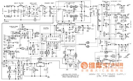
The rectifying and wave-filtering bridge, UR, commutation diode, VD1, VD2 and filter capacitor, C1 and C3. The switch control circuit consists of resistor, R2 and R4, voltage regulator diode, VS1 and field effect transistor, VF.
The voltage regulator circuit is composed of resistor R1, R3, R5, voltage regulator diode VS2, transistor, V, diode, VD3, filter capacitor C2 and three-terminal integrated regulator IC1 and IC2. (View) When it isbeingused, it`s not proper to take voltage from C5 directly. It`s imposible to allow short circuit happened, otherwise it`ll burn V1 and V2. Because when short circuit takes place, the electric currentin coil LO of flyback transformer B1 will increase rappidly.
The voltage of coil L1 and L2 increases to a rather high level. It gives back the electric currentin V1 and V2 increasing as well. It causes intensive positive feedback. Finally it burns out as the limitation of power consumption of V1 and V2. This feedback of circuit belongs to series circuit feedback. And it can openand protectcircuit. But when load is increased, the feedback is strenghened. What`s more, the frequency will decrease as the load increases. The internal resistance is rather small, so short circuit will burn pliotron very easily. (View) The switch D. C. regulated power supply circuit introduced in the example uses TWH8778 electronic switching IC and it has high work`s efficiency, its circuit is simple which is easy to manufature. The output voltage and current of the power supply circuit are +12V and 1A respectively. Work`s Principle of the CircuitThe switch D. C. regulated power supply circuit is composed of input converting circuit, switch output circuit and automatical voltage regulator circuit and it is showed as the picture 5-39.
The input converting circuit consists of mains switch S, mains transformer T, commutation diode VD1-VD4 and filter capacitor C1. The switch output circuit is composed of electronic switching intergrated circuit, IC, resistor R1, R2, diode, VD5, induction coil, L and capacitor C2, C3.
(View) VMOS switching power supply circuit diagram. Because of adopting voltage comparator 710, so the circuit issimpler than former. As shown, resistor R1, R2, R3 and regulator VDl, VD2 form divider regulator circuit, three groups of 5V, 6V and 18V are separated from 28V input voltage, they areused as the power supply; resistors R12, R13, capacitor C13, diodes VD6, VD7 and transistor VT3 constitute the power soft-start circuit. The moment of power turn on, the drive pulse width of VMOS tube VTl increases exponentially. when the comparator 710 cut off the drive pulse firstly, it can prevent the current of energy storage inductor too large.
When the switch VTl cut down, the output voltage of switching power supply continues to rise because the current of energy storage inductor 🔗 External reference
Related Circuits
High pressure alarm with high sensitivity. It detects high-voltage electric energy from 10kV at a distance of 2m or from low-voltage mains (AC 220V) at a distance of 0.3m. The alarm device is simple to manufacture, compact, and user-friendly....
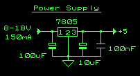
This circuit is a small +5V power supply, which is useful when experimenting with digital electronics. Small inexpensive wall transformers with variable output voltage are available from any electronics shop and supermarket. Those transformers are easily available, but usually...
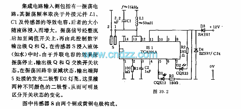
The integrated circuit input side contains an oscillating circuit, where the oscillation frequency is determined by the external components L1, C1, and the sensor's equivalent capacitance. The equivalent capacitance increases as the sensor is immersed in liquid. The oscillating...
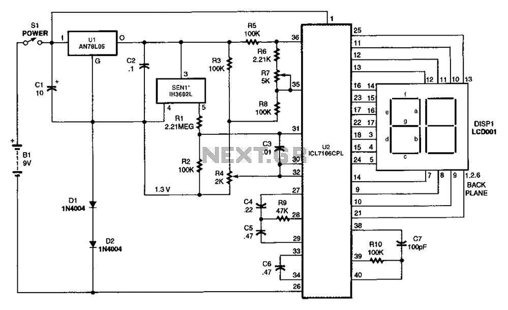
The output DC voltage of sensor SEN1 changes linearly in response to variations in relative humidity. This DC voltage is routed through resistors R1 and R2 to the analog-to-digital (A/D) converter chip U2. Resistor R4 is connected to ground,...

The circuit illustrated in Figure 3-132 represents an automatic round-trip plug braking circuit. To prevent or limit malfunctions of switch SQ1 and switch SQ2 that could lead to accidents, two additional protection limit switches, S03 and S04, have been...
When the comparator's output transitions from low to high, the rising edge of the output pulse, differentiated by the Cl/Rl chain, activates Ql. This action blocks the comparator via its strobing input and maintains its output state for a...
Warning: include(partials/cookie-banner.php): Failed to open stream: Permission denied in /var/www/html/nextgr/view-circuit.php on line 713
Warning: include(): Failed opening 'partials/cookie-banner.php' for inclusion (include_path='.:/usr/share/php') in /var/www/html/nextgr/view-circuit.php on line 713