
synthesized PLL for Low Power FM transmitter

The synthesized PLL circuit is a critical component in low-power FM transmitter designs, allowing for precise frequency control and stability. The architecture generally consists of a voltage-controlled oscillator (VCO), a phase/frequency comparator, and a loop filter. The VCO generates an output frequency that can be adjusted based on the input control voltage. The phase/frequency comparator compares the output frequency of the VCO with a reference frequency derived from the crystal oscillator. The output of the comparator is used to adjust the control voltage applied to the VCO, ensuring that the VCO frequency locks onto the desired frequency.
In this design, the use of a 5.12 MHz crystal reference is essential for achieving the required frequency steps. The selection of the R divider value (R=512) is crucial, as it determines how the reference frequency is scaled down to match the VCO frequency. This allows for finer frequency adjustments and ensures compatibility with the FM channel spacing requirements.
The prescaler (P=40) reduces the input frequency to a manageable level for the PLL, allowing it to function correctly within its specified input frequency range. The downconversion process is necessary because the phase/frequency comparator has a limited operating frequency range. By ensuring that the input frequency does not exceed 10 MHz or 15 MHz, the PLL can maintain accurate phase and frequency comparisons, leading to stable operation.
The flexibility of this PLL design enables it to be adapted for use in various applications beyond low-power FM transmission. By recalibrating the loop filter and VCO components, as well as adjusting the programming keys and crystal values, this circuit can be tailored to meet specific frequency stability and locking requirements for different systems.This is schematic of a synthesized PLL for the Low Power FM transmitter. By the way, you also can use it with other circuits, just pay attention to recalculate the loop filter response and components, VCO tank circuit, and the correct thumbswitch programming keys, crystal value. The original project of FM transmitter was made to operate in both co nfiguration ( synthesized or open loop free oscilattor), with synthesized version you can assure very high frequency stability, and also lock digital FM receivers ( 200KHz step in major of countries). A crystal reference of 5. 12 MHz was employed to assure 10 KHz steps ( enough sufficient to FM channeling of 200 KHz), and it also depends of R divider crystal reference, here I used R=512 to the MC145151P2 of Motorola.
P - is the prescaler divider, normally P=40 to MC12016, the PLL needs downconverter the input frequency ( pin1) because the phase/frequency comparator just work at maximum of 10MHz or 15MHz input frequency. 🔗 External reference
Related Circuits
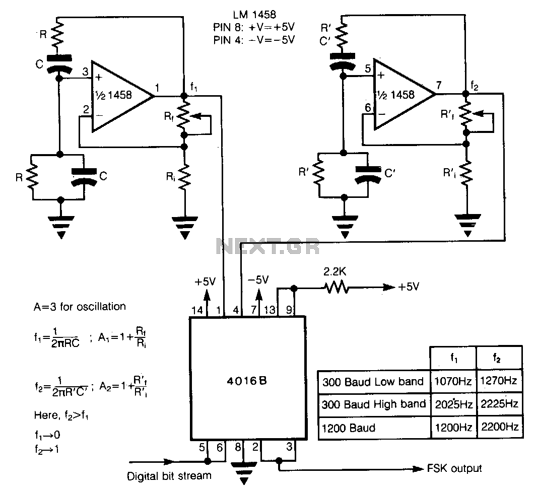
In Frequency Shift Keying (FSK), two distinct frequencies are utilized to represent the binary digits 0 and 1. The core of the circuit comprises two Wien-bridge oscillators constructed with a dual operational amplifier LM1458, each generating one of the...
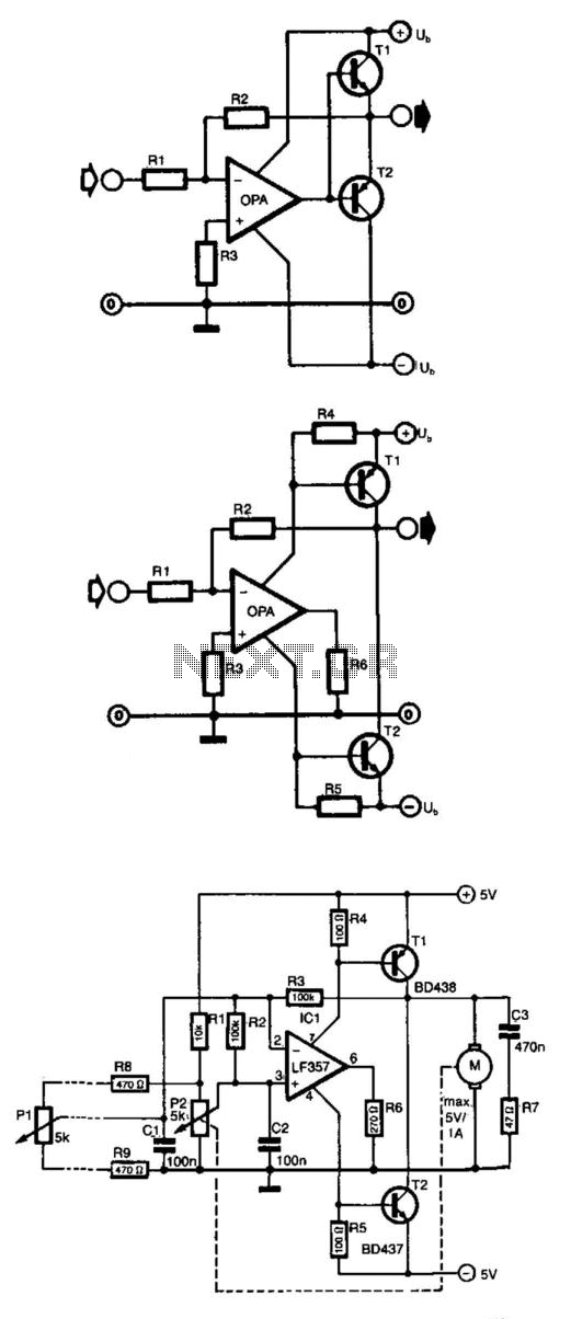
Frequently, the output current of an operational amplifier is inadequate for applications such as driving a small motor or loudspeaker. This issue is typically resolved by adding an emitter follower to the circuit. However, this configuration does not allow...
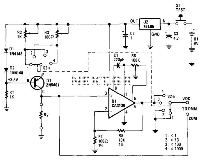
The circuit includes a 5-V regulator, a constant-current source (D1, D2, and Q1), and an operational amplifier (op amp) gain stage (U1). Power is supplied by a 9-V battery, which is regulated to +5 V DC by a three-terminal...
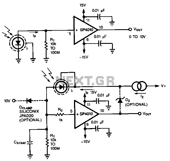
A common method of transforming the output current of a photodiode into a voltage signal involves paralleling the photodiode with a high-value load resistor, which results in a nonlinear response. Additionally, the combination of the load's transresistance, Rr, and...
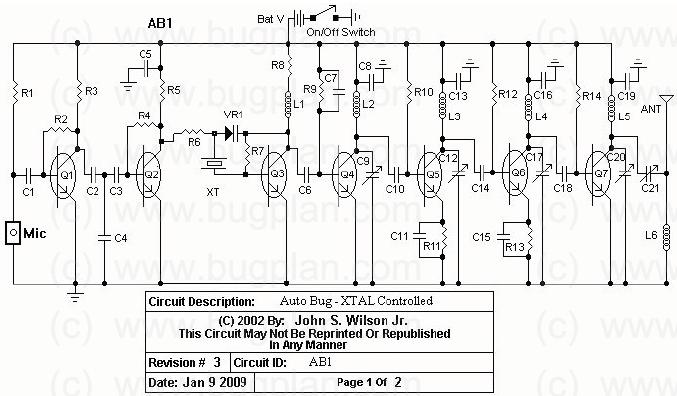
This circuit operates between 150 to 165 MHz. The crystals used are Digi-Key Electronics Barrel Crystals of the CA-301 type, which are relatively inexpensive. Any fundamental crystal with a frequency between 14 and 17 MHz can produce an output...
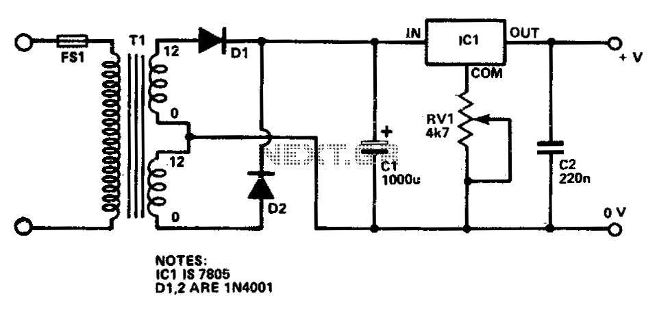
This circuit provides a regulated output voltage ranging from 5 V to 15 V DC, which can be adjusted using a preset resistor. The current output can reach up to approximately 350 mA. An integrated circuit is utilized to...