
TEMPERATURE REPORTING DIGITAL THERMOMETER

The circuit design involves the integration of read-only memory (ROM) or programmable read-only memory (PROM) modules that are essential for converting digital signals from the NE5037 temperature sensor. The NE5037 serves as an address line to access specific memory locations in the ROMs or PROMs, where the necessary conversion codes are stored. These codes are used to drive the segment display, which visually represents the temperature readings.
For temperatures ranging from 0 to 63 °F, the controller can directly utilize the output from the NE5037 to convert the sensor data into a readable format. However, when temperatures exceed 99 °F, an additional PROM must be incorporated to handle the hundreds digit. This additional component ensures that the display can accurately represent higher temperature values, thereby enhancing the system's functionality.
Furthermore, the design may include a timing mechanism, which could be realized using NAND gates or inverters. This clock circuitry is crucial for synchronizing operations within the system, ensuring that data is processed and displayed at the correct intervals. The use of NAND gates or inverters allows for a versatile and potentially cost-effective solution for generating clock signals, although the complexity of the circuit can increase based on the desired specifications and performance requirements.
Overall, the schematic will consist of the NE5037 interfacing with the ROMs or PROMs, the segment display for output, and the clock circuitry, all working in concert to provide accurate and timely temperature readings in degrees Fahrenheit. Proper attention to the logic design and component selection will ensure the reliability and efficiency of the temperature measurement system.The ROMs or PROMs must have the correct code for converting the data from the NE5037-used as address for the ROMs or PROMs-to the appropriate segment driver codes. The displayed amount could easily be converted to degrees Fahrenheit, °F, by the controller of (0 - 63 °temperature sensor) or through the (P) ROMs.
When doing this, a third (hundreds ) digit (P)ROM and display will be needed for displaying temperatures above 99 °F. An expensive clock can be made from NAND gates or inverters as shown. 🔗 External reference
Related Circuits
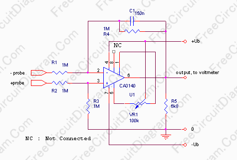
In some cases, a differential input is needed for voltage measurement. By using a single operational amplifier, it is possible to construct an adapter that provides a floating voltage reference. To achieve a differential input for voltage measurement using an...
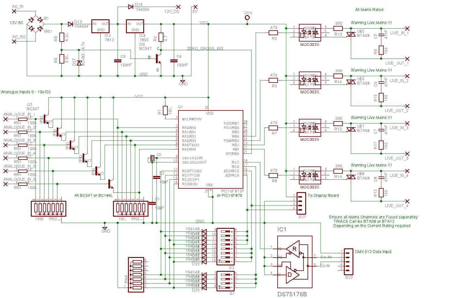
This unit receives DMX 512 data and Analogue (0-10V) data and uses these to phase angle control mains output. Features: DMX 512 data Input. Analogue (0-10V) DC Input. 4 Output channels. Remotely programmable Internally saved Presets. 3 Modes of...

The function is designed to automatically control the speed of a fan based on the temperature. Components include a BT136 Triac, capacitor, resistor, relay, and fan motor. The circuit employs a temperature sensing mechanism to monitor ambient temperature levels. A...
This circuit consists of a temperature sensor, amplifier, voltage-to-frequency (V/F) converter, a three-digit binary coded decimal (BCD) counter, a time base, and seven-segment LED displays. In addition to the 9400 V/F converter, other integrated circuits (ICs) required for this...
A digital clock project utilizing the PIC16C54 microcontroller can be constructed using the provided circuit diagram. This electronic project features a straightforward time-of-day clock that includes four seven-segment LED displays and three input switches, along with an additional reset...
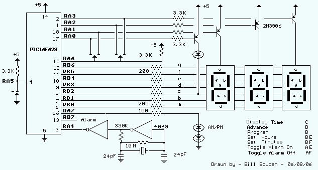
This clock timer uses a PIC16F628 microcontroller to display 3 and 1/2 digit time and control an external load. The clock includes a calendar with leap year and optional daylight savings adjustments. The timer output can be set from...