
The logic circuit diagram composed of photocoupler
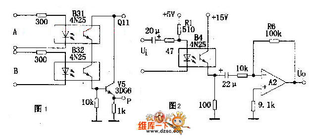
The AND gate logic circuit, as represented in Figure 1, is a fundamental building block in digital electronics. The output P of the circuit is high (1) only when both inputs A and B are high (1). This behavior is crucial for applications where a specific condition must be met before an output is triggered. The use of photodiodes in Figure B enhances the versatility of the circuit, allowing it to respond to light signals. When both photodiodes are illuminated, they conduct, enabling the output to reach a high state. This configuration can be adapted to create various logic gates, such as OR, NAND, and NOR gates, which are essential for constructing complex digital systems.
Figure 2 showcases an AC coupling amplifier circuit, designed to amplify alternating current signals while blocking direct current components. This circuit typically consists of an operational amplifier (op-amp), resistors, and capacitors. The coupling capacitors allow AC signals to pass while preventing DC bias from affecting the subsequent stages of the circuit. The design is particularly useful in applications where it is necessary to isolate the AC signal from any DC offset, such as in audio processing or light signal detection. The amplifier's gain can be adjusted by selecting appropriate resistor values, providing flexibility in signal amplification according to the specific requirements of the application.Figure 1 is AND gate logic circuit. Its logic expression is P=A, Figure B has 2 photodiodes in series. When input logic level A=1, B=1, output P=1. In a similar way, itcan form Or gate, NAND gate, NOR gate and some other logic circuits. As shown in figure 2, it is a typical AC coupling amplifier circuit, which is suitable for selecting lightin.. 🔗 External reference
Related Circuits

This is a design circuit for a low-cost FM antenna booster that can be used to listen to programs from distant FM stations clearly. The antenna FM booster circuit comprises a common-emitter tuned RF preamplifier wired around the VHF/UHF...
The concept of a color organ involves the transformation of sound, including musical tones, into light. According to wave theory, both music and light possess similar wave characteristics. A color organ is an electronic device that visually represents sound through...
The Delta configuration of resistors R2, R3, and R4 is converted to a Wye (Y) configuration. This conversion is necessary because a voltage divider is typically employed in series circuits. The aim is to determine the total resistance in...
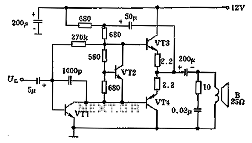
The overload protection circuit operates at a power of 650 mW with a supply voltage of 12 V and is designed for a speaker with an impedance of 25 ohms. The component specifications include: VT1 as transistor NB111EH/J, VT2...
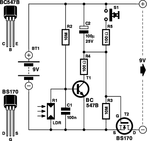
This is a small electronic switch that connects a battery to the equipment for a certain amount of time when a push-button is momentarily pressed. The ambient light level has also been considered; when it is dark, the display...
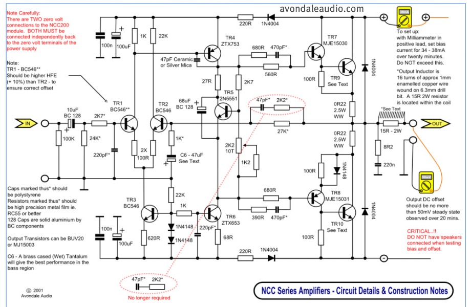
This is a simple circuit that features high-performance power amplifiers. The power amplifier is available as a PCB, along with a complete list of components. The described circuit utilizes high-performance power amplifiers, which are essential for applications requiring significant signal...