
The oscillator with electronic tuning of frequency

The oscillator circuit is designed to utilize a common-base transistor stage (Q1) for amplification, which is crucial for maintaining the oscillation process through positive feedback. The resistor R1 plays a pivotal role in determining the feedback signal's amplitude and, consequently, the overall gain of the circuit. The configuration of Q2 as a common collector allows for impedance matching, facilitating the connection of low-resistance loads without significant loss of signal integrity.
The frequency of oscillation is primarily dictated by the characteristics of the transistors involved and the inductive properties of coil L1. The design takes into account the variability of the oscillation frequency with respect to the supply voltage (Vcc). As the supply voltage increases, the transistors exhibit changes in conductivity, which directly affects the oscillation frequency. The observed behavior of the oscillator shows a decrease in frequency from 700 kHz to 420 kHz as the supply voltage ranges from 3 V to 9 V, indicating a strong dependency on the power supply.
The choice of the KT503d NPN transistor model is significant due to its specified parameters that ensure reliable performance within the desired frequency range. Key parameters such as saturation current (Is), current gain (Bf), and junction capacitances (Cjc and Cje) are optimized for high-frequency applications, making it suitable for this oscillator design. The circuit's layout and component values must be carefully selected to achieve the desired performance characteristics while maintaining stability and efficiency in operation.A schematic diagram of the oscillator is shown in Fig. 1. The common-base transistor stage (Q1) provides amplification of the signal in the positive feedback loop. The signal of the positive feedback develops across the resistor R1, this resistor is common to both the emitters of transistors Q1, Q2.
The transistor Q2 configured as common collector circuit. The frequency of oscillation is determined by the input and output conductance of transistors and the inductance of the coil L1. Both the frequency and amplitude of the oscillation depends on the value of the resistor R1. The frequency of oscillation changes in a wide range due to changes in the conductivity of the transistors when the supply voltage changes.
With the values of components, shown in fig. 1, the frequency of oscillator decreases from 700 kHz at Vcc = 3 V to 420 kHz at Vcc = 9 V (Fig. 2). To connect a low resistance load to the output of the oscillator it takes to use an emitter follower. . model KT503d NPN(Is=6. 843f Xti=3 Eg=1. 11 Vaf=129 Bf=106. 6 Ise=66. 48f Ne=1. 384 Ikf=. 8419 Nk=. 6328 Xtb=1. 5 Br=1. 2 Isc=26. 4p Nc=2. 088 Ikr=1. 637 Rb=6 Rc=1. 538 Cjc=23. 66p Mjc=. 33 Vjc=. 75 Fc=. 5 Cje=30. 84p Mje=. 33 Vje=. 75 Tr=648. 9n Tf=12. 74n Itf=1 Xtf=2 Vtf=30) 🔗 External reference
Related Circuits
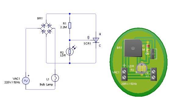
Adjust the value of R1 to achieve optimal performance of the LDR sensor. If, in practice, a resistance of 2.2 MΩ still activates the lamp, it is possible to increase the value of R1 to a larger resistance of...
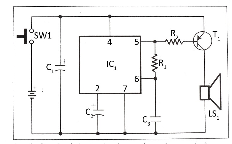
This document presents a verified circuit diagram for a simple, interesting, and cost-effective electronic clapper (sound generator) circuit, along with a description of its functionality. The electronic clapper circuit is designed to activate sound generation through the detection of sound...
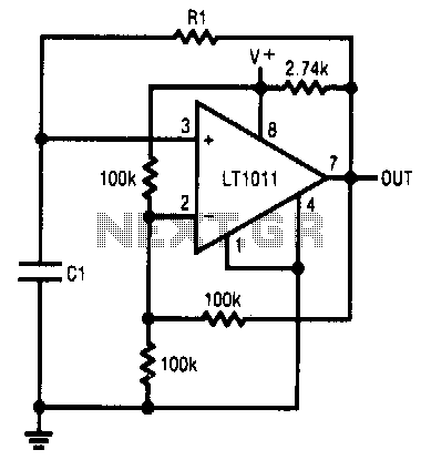
This simple RC oscillator utilizes a medium-speed comparator with hysteresis and feedback through R1 and C1 as timing elements. The frequency of oscillation is theoretically independent of the power supply voltage. Additionally, the comparator swings to the supply rails...
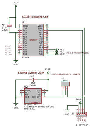
The SX 28 internal oscillator is not that fast, so an external oscillator can be hooked up to the processor as shown in the diagram to increase the operation cycles per second. The SX 28 microcontroller is designed with an...
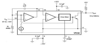
The circuit diagram of a voltage-to-frequency (V/F) converter is presented, designed to handle negative input voltage. It employs the VFC32 voltage-to-frequency converter, which is commonly utilized in various applications. The V/F converter circuit is essential in converting an analog voltage...
This is the circuit diagram for an electronic door lock security key system. This security system circuit combines a pressed key mechanism (non-mechanical), and the output can be connected to drive a relay to unlock the door. The electronic door...