
Three-channel tone control

The circuit described operates as a signal processing system, where the input signal is first buffered and amplified by IC1, ensuring that the characteristics of the input signal are preserved while preventing loading on the subsequent stages. The non-inverting amplifier configuration allows for a straightforward gain setting, which is crucial for maintaining signal integrity.
Following the amplification stage, the output is processed through three frequency shaping networks. These networks are essential for tailoring the frequency response of the overall circuit. Each network is associated with a variable resistor (RV1, RV2, RV3), which allows for real-time adjustments to the frequency characteristics of the signal. This flexibility is particularly useful in applications requiring fine-tuning of frequency response, such as audio processing or filtering applications.
The output from these networks is then fed into IC2, which functions as an inverting operational amplifier. The feedback path from the output of IC2 back to its inverting input is influenced by the three frequency shaping networks, allowing for precise control over the gain and frequency response of this stage. The design choice of using variable resistors in the feedback path enables dynamic adjustment of the circuit's performance, accommodating various operational requirements.
Overall, this circuit design exemplifies a modular approach to signal processing, where each stage is carefully designed to optimize performance while maintaining flexibility in the adjustment of frequency response. The interaction between the non-inverting amplifier and the inverting amplifier, along with the frequency shaping networks, creates a robust system capable of handling a wide range of signal processing tasks.The iriput signal is fed via SKI to the first active stage built around ICl. Configured as a noninverting amplifier whose gain is set by the ratio of R3 and Rl. In this case, the gain is set at unity. This initial stage is required to isolate the following stage from any loading effects. The output from ICl is fed via three frequency shaping networks to IC2 The three networks built around RV1, RV2, and RV3 are also included in the feedback path of IC2, another inverting op amp stage. The components associated with the three variable resistors are chosen to give the required frequency control.
Related Circuits
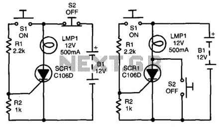
In both circuits, the SCR (Silicon Controlled Rectifier) and the lamp can be latched on by momentarily closing switch S1, which provides gate drive to the SCR through resistor R1. In both configurations, the gate is connected to the...
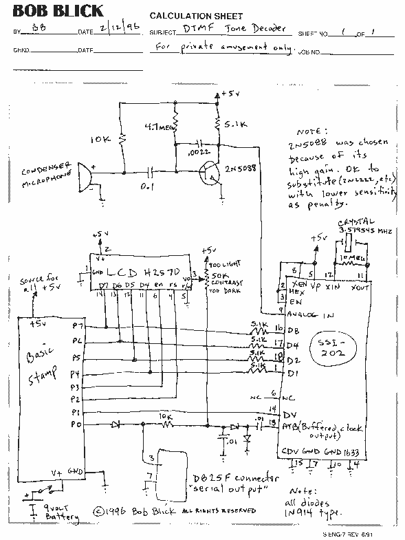
This project displays telephone numbers decoded from tones. A microphone picks up the tones, a preamplifier boosts the signals, an SSI-202 DTMF chip decodes the tones, a Basic Stamp acts as an interface to an LCD display and also...
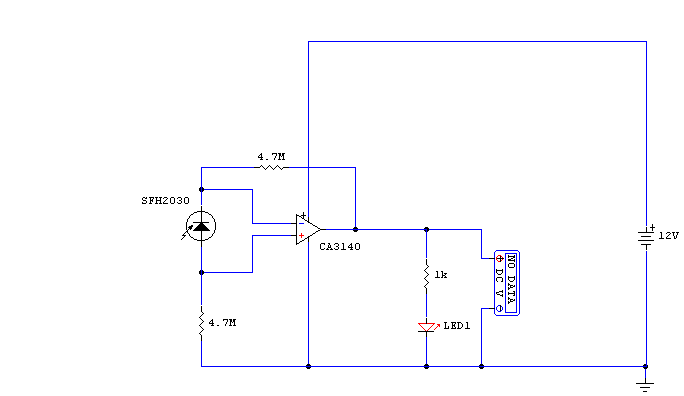
While developing an infrared (IR) extender circuit, a method was required to measure the relative intensities of different infrared light sources. This circuit is the culmination of that research. It utilizes a photodiode, specifically the SFH2030, as the infrared...
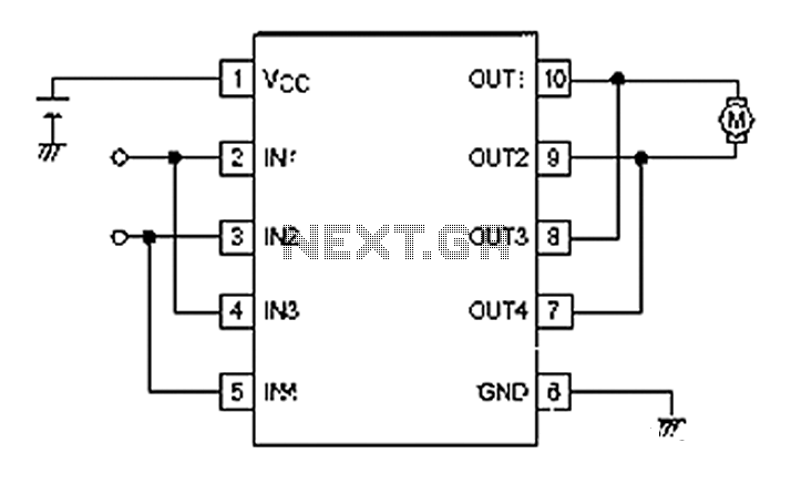
A simple motor control project for forward and backward drive can be implemented using the LB1948M motor driver IC, which features two channels for motor control. The LB1948M is an ideal choice for 12V motor drive systems and can...
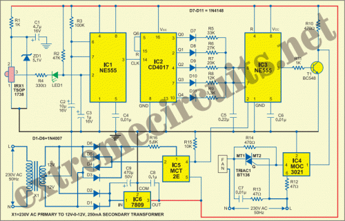
This circuit allows for the adjustment of fan speed from a distance, such as from a couch or bed. It utilizes the TSOP1738 infrared receiver module to capture the infrared signals. The circuit operates by employing an infrared remote control,...
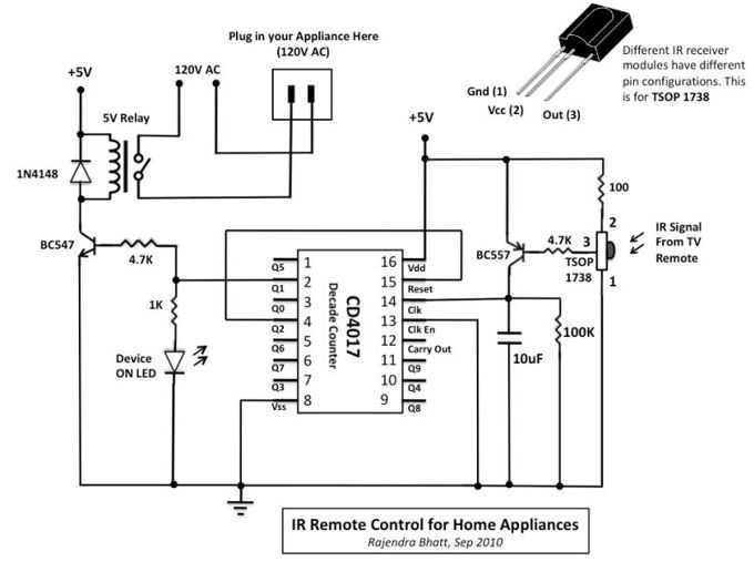
The infra-red (IR) toggle switch project described here is aimed to provide control mechanism for electrical appliances that do not have remote operation features. The goal is to construct a black box where you can plug-in your 120V AC...