
thyristor trigger circuit schematic diagram

The described circuit operates by utilizing a zero-crossing detector, which is designed to identify the point at which an alternating current (AC) signal crosses zero volts. This detection results in a pulse that transitions from low (0) to high (1) and back to low (0). This pulse serves as a trigger for the R-S flip-flop, a fundamental digital memory element that can store a single bit of information.
Upon receiving the pulse from the zero-crossing detector, the R-S flip-flop is set, which enables it to enter a state where it can control subsequent components in the circuit. The output of the flip-flop is connected to the ramp circuit, denoted as "A to Ramp." This connection activates the ramp circuit, allowing it to begin generating a linear voltage ramp over time.
The ramp circuit typically comprises a resistor-capacitor (RC) network, which determines the rate of ascent of the voltage ramp. The values of the resistor and capacitor are selected based on the desired timing characteristics of the circuit. As the ramp circuit operates, it produces a gradually increasing voltage that can be used for various applications, such as timing, waveform generation, or triggering other circuits.
In summary, this circuit effectively utilizes a zero-crossing detector to provide a precise timing signal that controls the operation of an R-S flip-flop, which in turn initiates a ramp circuit. The design ensures reliable timing and voltage control for various electronic applications.The circuit takes its input from the "zero-crossing detector", which provides it with a 0-to-1-to-0 pulse to "set" the R-S flip-flop and release the ramp circuit (A to Ramp) for it to start the ascent of the timing ramp. 🔗 External reference
Related Circuits
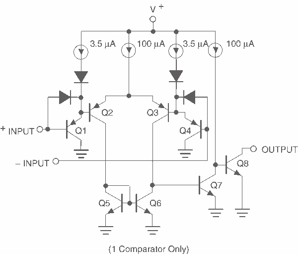
This page provides basic information about voltage comparator integrated circuits and is to act as reference material for other circuits. The circuits shown are based on the LM339 Quad Voltage Comparator chip or the LM393 Dual Voltage Comparator chip....
%2Band%2B(US)%2BCX500%2BC%2B1979-81%2Band%2B1979%2BCX500%2BD%2BElectrical%2BWiring%2BDiagram.jpg)
Lamp Electrical Circuit Diagram Manual PDF Download. This document provides a comprehensive manual for downloading the electrical circuit diagram of a lamp. The circuit diagram serves as a crucial reference for understanding the electrical connections and components involved in lamp...
This infrared alarm barrier is designed to detect individuals passing through doorways, corridors, and small gates. The transmitter emits a beam of infrared light that is invisible to the human eye. When the light beam is interrupted by a...
The recommended transmitter is straightforward to construct and suitable for beginners. Despite its simple design and compact size, it delivers remarkable performance. It operates for 12-15 hours on a 9-volt battery and has a transmission range of 100 to...

The adjustable voltage monitor can be used to check whether the voltage in a circuit remains within a given range. If the DC voltage is less than the voltage at pin 5 of U1-B, then LED1 will light. If...

Transistors are essential components of electronic circuits. The success of a circuit design depends on the selection of the appropriate transistor type and the calculations involved. Transistors serve as fundamental building blocks in electronic circuits, playing critical roles in amplification,...