
Tone-burst oscillator and decoder

In this circuit, the tone burst serves as a synchronization signal that facilitates the establishment of communication between the transmitter and receiver. The phase-locked loop (PLL) is a crucial component in this setup, as it is responsible for demodulating the incoming tone burst signal. The PLL locks onto the frequency of the tone burst, ensuring that the receiver can accurately decode the information contained within the signal.
Once the PLL successfully locks onto the tone burst, it produces a corresponding output signal at pin 3 of the logic gate. This output is typically a digital signal that transitions from a low to a high state, indicating that the tone burst has been successfully detected. The logic gate processes this signal and generates a control signal that is used to activate the carrier-operated switch (COS).
The COS is designed to control the flow of power to a load or another part of the circuit based on the presence of the tone burst signal. When the output from the logic gate goes high, the COS is turned on, allowing current to flow through the circuit and enabling the connected device to operate. This mechanism is essential for ensuring that the device only activates in response to the correct tone burst, thereby preventing unintended operation due to noise or other signals.
Overall, this configuration is widely used in communication systems where reliable signal detection and control are paramount. The use of a PLL for decoding the tone burst enhances the robustness of the system, making it less susceptible to interference and improving the overall performance of the transmission.A tone burst sent at the beginning of each transmission is decoded (at receiver) by a PLL causing output from pin 3 of logic gate to turn on carrier-operated switch (COS).
Related Circuits
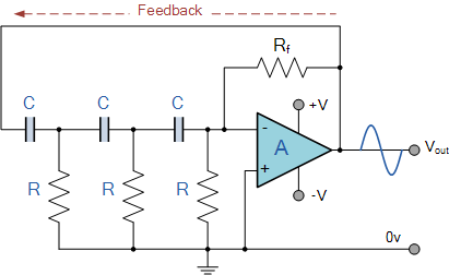
Electronics tutorial about the RC oscillator circuit, RC phase shift oscillators, and how a tuned RC oscillator circuit produces sine waves. The RC oscillator circuit is a fundamental electronic circuit used to generate oscillating signals, particularly sine waves. This circuit...

This circuit functions as a universal decoder, capable of operating either as a dual 1-of-4 decoder or as a single 1-of-8 decoder, depending on the signal applied to the Mode Control (M) input. In the dual mode, each section...
The RF design and construction of radio frequency oscillators. Radio frequency (RF) oscillators are essential components in various electronic systems, generating signals at specific frequencies used for communication, signal processing, and other applications. The design of RF oscillators involves several...
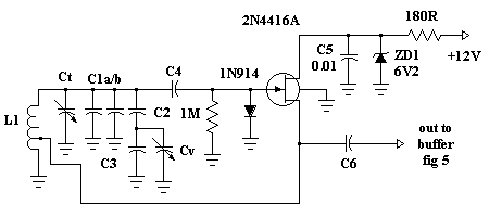
In the circuit, the frequency trimming component is configured such that the voltage across it is in quadrature with the voltage V0 from the bridge. This arrangement allows for adjustments to be made with minimal changes to the attenuation...
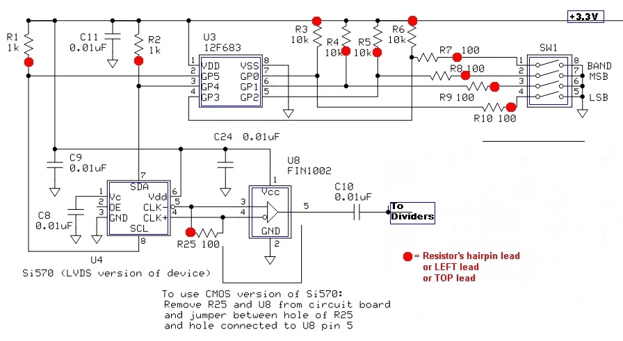
The current draw should be between 80 and 100 mA. The exact value is highly dependent on the Si570, its version (CMOS vs. LVDS), the frequency setting, and variations in the circuit components. The SW1 programming of U3 can...
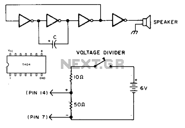
This simple circuit utilizes the 7404 low-power Schottky hex inverter. Capacitor C is a 5 to 30 µF electrolytic capacitor selected for the desired pitch. The speaker is a 2-inch, 8-ohm unit. The circuit employs a 7404 low-power Schottky hex...