
Touch Switch And Delay Circuit

The circuit operates using a 555 timer IC configured in monostable mode, which is ideal for generating a single output pulse in response to a trigger event. The touch switch functionality allows for user interaction, enabling the circuit to be activated by a simple touch. The output pulse duration is primarily determined by the resistor R3 and capacitor C2 values, which define the RC time constant.
When the circuit is triggered by a touch, the voltage at the trigger pin (pin #2) drops below the threshold level (Vcc/3), causing the 555 timer to switch its output from low to high. This transition activates the charging process of capacitor C2 through resistor R3. The exponential charging behavior of C2 means that the voltage across it rises gradually, and the time it takes to reach 2Vcc/3 determines how long the output remains high.
Once VC2 reaches the threshold level of 2Vcc/3, the internal comparator resets the flip-flop, which in turn turns on the discharging transistor, allowing C2 to discharge. This discharging process causes the output to revert to low. The cycle then repeats, allowing for continuous operation as long as the circuit is powered and triggered appropriately.
Adjustments to the timing characteristics can be made by changing the resistor and capacitor values. For instance, increasing R3 or C2 will extend the pulse duration, while decreasing either component will shorten the delay. This flexibility makes the circuit suitable for various applications where a timed response is required, such as in delay circuits, timers, or simple control systems.
Overall, the simplicity and effectiveness of the 555 timer in monostable mode make it a popular choice for creating touch-activated circuits with adjustable timing capabilities.This is a simple touch switch circuit, the 555 timer is configured as a one shot multivibrator that is triggered by touching the touch terminal. In this monostable mode, the timer generates a fixed pulse of about 4 seconds whenever the trigger voltage falls below Vcc/3.
When the trigger pulse voltage applied to the #2 pin falls below Vcc/3 while th e timer output is low, the timer`s internal flip-flop turns the discharging Tr. off and causes the timer output to become high by charging the external capacitor C2 and setting the flip-flop output at the same time. The voltage across the external capacitor C2, VC2 increases exponentially with the time constant t=R3*C2 and reaches 2Vcc/3 at td=1.
1R3*C2. Hence, capacitor C2 is charged through resistor R3. The greater the time constant, the longer it takes for the VC2 to reach 2Vcc/3. In other words, the time constant R3*C2 controls the output pulse width. When the applied voltage to the capacitor C2 reaches 2Vcc/3, the comparator on the trigger terminal resets the flip-flop, turning the discharging Tr. on. At this time, C2 begins to discharge and the timer output converts to low. In this way, the timer operating in the monostable repeats the above process. To increase the time of the delay from 4 seconds, the value of R3 and C2 need to be increased. Similarly, to decrease the output time delay, the value of R3 and C2 need to be reduced. 🔗 External reference
Related Circuits
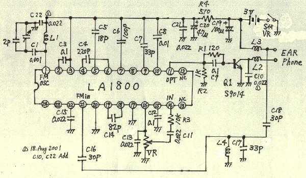
Earphones, batteries are sold separately. AM / FM seems to be a common mold. But stamping is different. AM / FM E193577 UL94V0 board with the AM / FM etching printed circuit board manufacturers are the same. Shape is...
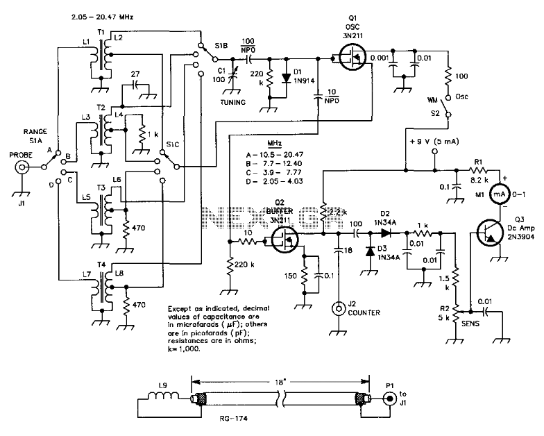
This circuit is designed for checking resonances in tuned circuits, antennas, and similar applications, covering a frequency range of 2 to 20 MHz. Q1 acts as an oscillator that can be tuned across this range using capacitor C1 and...
A recent thrift shopping experience revealed a toy that appears to be suitable for circuit bending. The toy was found without batteries, preventing any testing at the store. It may be beneficial to bring batteries during future visits or...
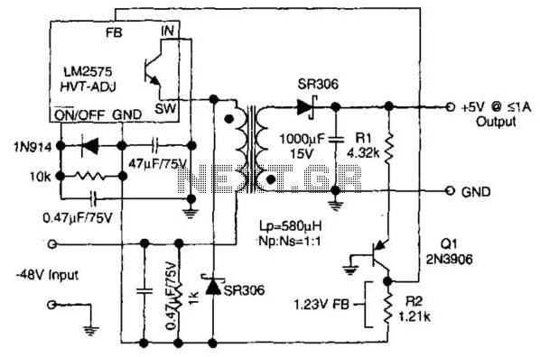
The circuit supplies 1 A at +5 V from the -48 V supply commonly used in telephone equipment. More: The National Semiconductor LM2575 is a simple switching regulator. The circuit utilizes the National Semiconductor LM2575, which is a step-down (buck)...
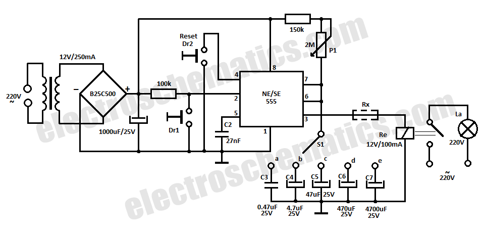
This time delay relay circuit is constructed using the NE/SE555 integrated circuit, manufactured by Intersil, which features a precision timer. The circuit exhibits stability against temperature variations. The NE/SE555 integrated circuit is a versatile timer used in various applications, including...
Feedback in a public address amplifier should be avoided. The ideal solution is to adjust the positions of the microphone and speaker; however, this is not always feasible in many situations. A frequency shifter that alters the output frequency...