
TUNED-COLLECTOR ARMSTRONG OSCILLATOR
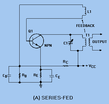
The described circuit presents a fundamental configuration for generating oscillations through the use of an Armstrong oscillator. In this arrangement, the DC path is critical for biasing the transistor Q1, which acts as the active component of the oscillator. The resistor RE serves as an emitter resistor, providing stability and setting the operating point of Q1.
The tank circuit, which consists of an inductor and a capacitor, is crucial for determining the oscillation frequency. The AC component generated by the transistor Q1 is fed into the tank circuit, where it resonates at a specific frequency determined by the values of the inductor and capacitor. This resonance is essential for sustaining oscillations.
The modification to create a shunt-fed, tuned-collector configuration involves routing the output from the collector of the transistor back into the tank circuit while ensuring that the DC component is effectively blocked by capacitor C2. This capacitor acts as a coupling device, allowing only the alternating current (AC) signals to pass through to the tank circuit while preventing any DC bias from affecting the oscillation process.
In summary, the circuit operates by utilizing the transistor's ability to amplify signals, with the tank circuit providing the necessary conditions for oscillation. The careful arrangement of components ensures that the oscillator functions effectively, producing a stable output signal characterized by its frequency and amplitude. Proper selection of the inductor and capacitor values, alongside the biasing of the transistor, is essential for achieving optimal performance in this configuration.The dc path is from the negative side (ground) of VCC through RE, Q1, T1, and back to the positive side of VCC. The figure clearly illustrates that both the ac and dc components flow through the tank circuit. By modifying the circuit slightly, it becomes a SHUNT-FED, TUNED-COLLECTOR ARMSTRONG OSCILLATOR as shown in view (B). The dc component flows from ground through RE to Q1 to positive VCC. The dc is blocked from the tank circuit by capacitor C2. Only the ac component flows in the tank circuit. 🔗 External reference
Related Circuits
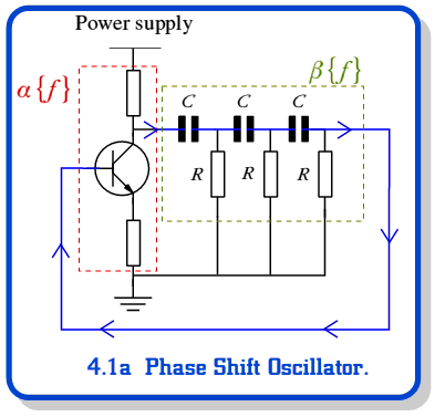
A feedback oscillator employs positive feedback to sustain oscillation. Essentially, an oscillator functions as an amplifier that incorporates feedback. A feedback oscillator is a critical component in various electronic applications, utilizing the principle of positive feedback to generate continuous waveforms....
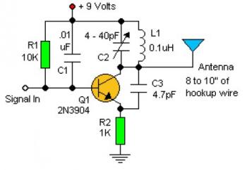
Experimenting with the size of the coil and the number of turns can influence the frequency and signal output of the oscillator. The signal can be received using a standard FM radio receiver. The input signal should be coupled...
This circuit generates a low power test signal and should not be used as a transmitter. Make sure you are within the law in the locality in which you operate this. As this was built from parts laying on...
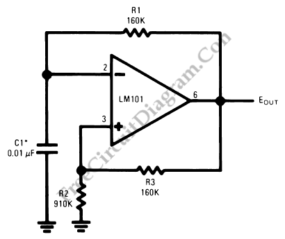
This is an operational amplifier (Op-Amp) oscillator circuit. This circuit has several advantages, including its ability to operate at low frequencies. The operational amplifier oscillator circuit is designed to generate a periodic waveform output, typically a sine or square wave,...
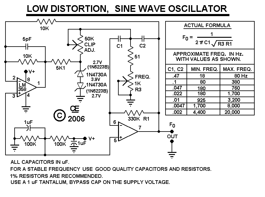
After constructing the device, adjust the frequency to the desired level using the "Frequency Control." Then, utilize an oscilloscope to fine-tune the waveform for optimal performance with the "Clip Control." The sharp rise and fall times of square waves...
Several NPN transistors can oscillate within the audio frequency range when reverse biased. The minimum supply voltage required is 7V for low-power transistors like the BC109, BC238, and 2N2222A; it increases to 12V for medium-power transistors such as the...