
TV transmitter circuit
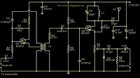
The TV transmitter circuit operates by employing frequency modulation (FM) techniques for audio signals and phase-alternating line (PAL) standards for video signals. The initial stage involves the pre-amplification of the audio input through transistor Q1, which is configured to enhance the audio signal to a suitable level for further processing. This transistor is typically biased to operate in its active region, ensuring linear amplification.
Transistor Q2 plays a crucial role in the modulation process. It is configured to operate in a common-emitter configuration, which allows it to modulate the audio signal onto the carrier frequency generated by the tank circuit. The tank circuit, consisting of capacitor C5 and inductor L1, is tuned to resonate at the desired carrier frequency. The values of C5 and L1 must be selected carefully to achieve the correct frequency, which is essential for effective transmission.
The video signal, which is typically a composite signal, is fed into the emitter of transistor Q2 through potentiometer R7. The potentiometer allows for adjustment of the video signal level, ensuring that the modulation of the video does not distort the audio signal. This adjustment is critical for maintaining the integrity of the transmitted signal.
Once the audio and video signals are modulated, the composite output is transmitted via antenna A1. The antenna must be designed to operate efficiently at the chosen transmission frequency, ensuring that the signal can be effectively radiated over the desired coverage area.
Overall, this TV transmitter design incorporates essential components and configurations that enable the successful modulation and transmission of audio and video signals, adhering to established broadcasting standards. Proper component selection, biasing, and tuning are key factors in achieving optimal performance in this circuit.The TV transmitter given here uses UK standard 1 FM modulation for sound and PAL for video modulation. The audio signal to be modulated is pre-amplified using the transistor Q1 and associated components. The transistor Q2 has two jobs: production of carrier frequency and modulation. The pre-amplified audio signal is fed to the base of transistor Q 2 for modulation. Capacitor C5 and inductor L1 forms the tank circuit which is responsible for producing the carrier frequency. The video signal is fed to the emitter of transistor Q2 via POT R7 for modulation. The modulated composite signal (audio+video) is transmitted by the antenna A1. 🔗 External reference
Related Circuits
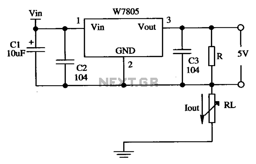
The circuit is composed of a W7805 positive current source application integration circuit that includes a voltage regulator. The W7805 regulator operates in suspension. A resistor is placed between its output terminal and the common terminal, forming a constant...
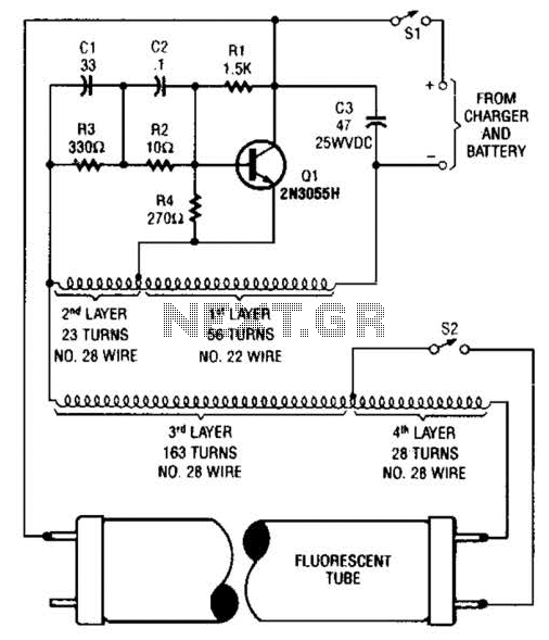
A 2N3055 oscillator (Q1) drives a homemade transformer, wound on a Vk ferrite rod. S2 is used as a filament switch and can be eliminated if desired. A 20-W fluorescent tube is recommended. The supply voltage is 12 V. The...
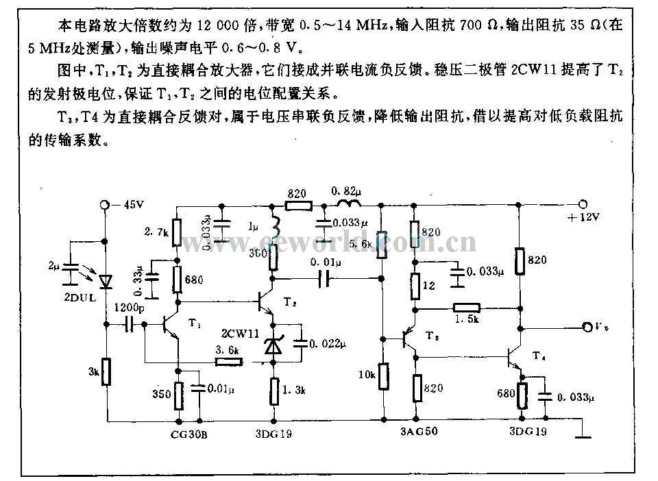
The amplification of this circuit is approximately 12,000 times, with a bandwidth ranging from 0.5 to 14 MHz. The input resistance is 700 ohms, while the output resistance is 35 ohms (measured at 5 MHz). The output noise level...
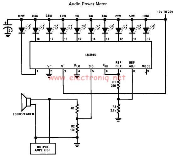
The LM3915 monolithic integrated circuit can be used to design a simple audio power level meter that senses analog voltage levels and drives ten LEDs, LCDs, or vacuum fluorescent displays, providing a logarithmic 3 dB/step analog display. One pin...
The Ai. A2 series operates with a telephone line, where sound anomalies or off-hook currents activate a light within an arc tube, which in turn triggers a photosensitive MOSFET. This process involves a saturated conduction base voltage that sends...
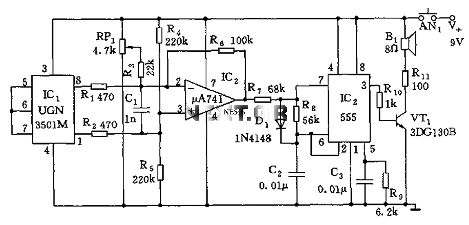
The circuit consists of a 555 timer and associated components designed for voltage-to-frequency conversion. It is utilized for determining the orientation of Earth's magnetic field using a Hall-effect sensor, specifically the UGN-3501M. This sensor incorporates a Hall element and...