
tv transmitter circuit
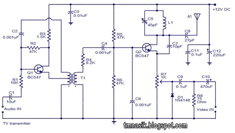
The described TV transmitter circuit is designed to function effectively within the parameters of UK broadcasting standards, ensuring compatibility with existing television reception systems. The use of FM modulation for audio allows for a robust transmission, minimizing noise and interference, which is critical for maintaining sound quality. The PAL video modulation is standard for video broadcasting, ensuring that the transmitted video signal adheres to established formats for compatibility with TV receivers.
Transistor Q1 operates as a preamplifier, boosting the audio signal before it is fed into the modulation stage. The choice of components around Q1, such as resistors and capacitors, is crucial for setting the gain and frequency response of the audio signal, which directly influences the quality of the transmitted sound.
Transistor Q2 not only modulates the audio signal but also generates the carrier frequency necessary for transmission. The tank circuit, consisting of capacitor C5 and inductor L1, is tuned to resonate at the desired frequency, which is vital for effective signal transmission. The careful selection of these components affects the stability and efficiency of the carrier generation.
The inclusion of potentiometer R7 allows for fine-tuning of the video signal level before it is fed into the modulation stage. This adjustability is essential for achieving the right balance between the audio and video components, ensuring that neither overwhelms the other in the composite output.
The antenna A1 plays a critical role in transmitting the modulated signal over the airwaves. The design and placement of the antenna can significantly affect the transmission range and quality of the received signal.
Power supply considerations are also paramount in this circuit. A stable 12V DC supply is necessary to ensure consistent operation of the circuit components. The recommendation to use a battery highlights the importance of reducing electrical noise, which can interfere with the modulation process and degrade the quality of the transmitted signal. A well-regulated power supply is essential if a DC power source is used, as fluctuations in voltage can lead to performance issues.
Overall, this TV transmitter circuit represents a comprehensive approach to broadcasting, incorporating essential electronic principles and components to achieve effective transmission of audio and video signals.The TV transmitter circuit given here uses UK standard 1 FM modulation for sound and PAL for video modulation. The audio signal to be modulated is pre-amplified using the transistor Q1 and associated components. The transistor Q2 has two jobs: production of carrier frequency and modulation. The pre-amplified audio signal is fed to the base of tran sistor Q2 for modulation. Capacitor C5 and inductor L1 forms the tank circuit which is responsible for producing the carrier frequency. The video signal is fed to the emitter of transistor Q2 via POT R7 for modulation. The modulated composite signal (audio+video) is transmitted by the antenna A1. This TV transmitter circuit can be operated from 12V DC. Either a 12V DC power supply or a battery can be used for the purpose, using a battery will surely reduce noise and improve the performance.
If you are going with a DC power supply, then it must be well regulated and free of noise. 🔗 External reference
Related Circuits
The IR Theremin hardware schematic is notably simple, as the primary input and output devices require minimal connections. This simplicity can be a double-edged sword, as fewer hardware components often lead to increased software complexity. The main components utilized...
The LM555 timer IC can be utilized in various electronic projects, including the creation of an analog timer. According to the datasheet, the LM555 is versatile and can be adjusted to set timers based on specific requirements. The schematic...
The 220V AC mains supply is downconverted to 9V AC by transformer X1. The transformer output is rectified by diodes D1 through D4 wired in bridge configuration, and the positive DC supply is directly connected to the charger's output...

This is a design circuit for a low-cost FM antenna booster that can be used to listen to programs from distant FM stations clearly. The antenna FM booster circuit comprises a common-emitter tuned RF preamplifier wired around the VHF/UHF...
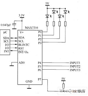
The main technical characteristics of the MAX7316 include a 400 kbps, 2-wire serial interface with a voltage tolerance of 5.5V. The operating voltage ranges from 2V to 3.6V. It features 8-bit PWM control for white LED brightness, with global...
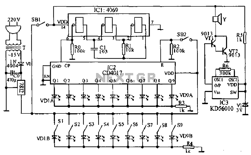
This document presents a principle circuit for electronic games. The main circuit operates in conjunction with the host through the reset button SB2, while the indicators VD1A-VD9A remain off. Prizes, for example, five, are determined by the number of...