
Understanding LVDS Fail-Safe Circuits
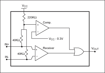
The LVDS (Low-Voltage Differential Signaling) receiver is a critical component in high-speed data communication systems, where maintaining signal integrity is essential. The failsafe function is designed to ensure that the output remains stable and predictable, even when the input connections are compromised. This is particularly important in applications where signal integrity is paramount, and any ambiguity in output could lead to erroneous data interpretation.
Three prevalent failsafe methods are discussed in this context:
1. **External Biasing**: This method involves adding a biasing circuit external to the LVDS receiver. The external biasing circuit typically consists of resistors and a voltage source, which ensures that the receiver's output defaults to a known state (usually a logic high or low) when no valid input signal is present. This approach offers flexibility in configuring the failsafe state but may require additional components and PCB space.
2. **In-Path Failsafe**: In this configuration, the failsafe mechanism is integrated directly into the signal path of the LVDS receiver. This can be achieved through the use of specific resistive networks or active devices that detect the absence of an input signal and automatically drive the output to a predetermined state. This method reduces component count and simplifies the design but may introduce additional complexity in the signal path.
3. **Parallel Failsafe**: This technique involves connecting a secondary circuit in parallel with the main signal path. The parallel circuit monitors the input signals and, in the absence of valid data, overrides the output to a defined state. This method can provide redundancy and improve reliability but may also increase power consumption and require careful design considerations to avoid interference with the main signal.
Each of these failsafe functions has distinct advantages and trade-offs, making it essential to select the appropriate method based on the specific requirements of the application, such as cost, complexity, and performance criteria. Understanding these characteristics allows engineers to design robust LVDS systems that maintain signal integrity and reliability under various connection conditions.LVDS receiver needs a failsafe function to avoid uncertain output state when it has an improper connection. In this appnote, we examine the circuits and characteristics of three popular failsafe functions: external-biasing, in-path, and parallel..
🔗 External reference
Related Circuits
The 555 limit circuit, which is an integrated electrical circuit, is designed to manage large electrical loads. It automatically disconnects power when the load exceeds a predetermined threshold. Once the load is reduced below this threshold, power is restored...
Do not drink and drive. Wishing you a safe journey home. Language Integrated Circuits. Language Integrated Circuits (LICs) are specialized electronic components designed to facilitate the processing of language-based data within various applications. These circuits integrate multiple functions, such as...
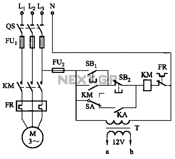
The circuit illustrated in Figure 3-81 employs a transistor delay circuit to facilitate start-stop cycle control. It can operate in both manual and automatic modes. The circuit is primarily governed by the motor run time circuit, which includes transistors...
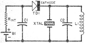
Leo Esaki invented the tunnel diode in 1957 while working at Sony (then known as Tokyo Tsushin Kogyo). Tunnel diodes feature a very narrow, heavily doped p-n junction approximately 10 nm wide, which exhibits a broken bandgap. This configuration...
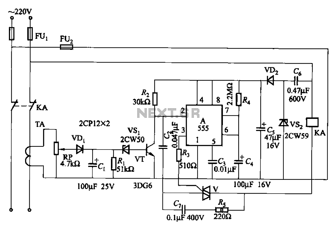
This circuit is a simple -5V power supply using a 555 timer, designed for low-power analog applications involving FET operational amplifiers. The circuit converts +5V to -5V to create a dual power supply. It operates as a 555 astable...
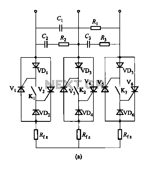
Figure 16-48 (a) illustrates the introduction of a six thyristor three-phase AC switching circuit, while Figure 16-48 (b) depicts the implementation of three triac circuits. These configurations are suitable for motors and other inductive loads. The six thyristor three-phase AC...