
USB Live Oscilloscope: Clock Generator
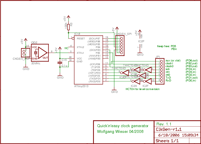
The circuit design employs an ATtiny2313 microcontroller, which operates at 20MHz to generate a stable 10MHz sampling clock. This clock is critical for driving an analog-to-digital (AD) converter and latches, ensuring consistent data acquisition. The use of HCT04 inverters facilitates the necessary level shifting, permitting integration with other digital logic that operates at lower voltage levels. The CKGEN_SPI connector is essential for in-system programming, providing a straightforward means to upload firmware to the ATtiny2313, which is responsible for managing the clock generation and write strobe timing.
The sampling clock's stability is paramount, as it also serves as the USB interface clock (USB_IFCLK) for the USB-FX2 board. Any fluctuation in this clock signal could disrupt data flow, as evidenced by previous debugging efforts that identified glitches caused by improper synchronization in the firmware. The design's flexibility allows for various sampling rates by controlling the write strobe signals on clock1, enabling dynamic adjustment of data throughput as dictated by application requirements.
The firmware development process is critical, requiring meticulous attention to timing specifications to ensure that the sampling clock remains synchronized with the write strobes. This synchronization is achieved through the use of an on-chip timer/counter, which must be precisely calibrated to maintain the integrity of the data being processed. Overall, this circuit configuration provides a robust solution for generating variable sampling clock write strobe pulses while ensuring compatibility with existing digital logic and maintaining high data integrity over USB.Produce the varying sampling clock write strobe pulses. So, I settled with this semi-optimal but working design applying an ATtiny2313 microcontroller from Atmel. For a 10MHz sampling clock, I need a 20MHz clock for the ATtiny2313and hence it needs to be powered at 5V instead of 3.
3V like all the other logic around. So, I had to add these HCT04 inverters for logic level translation of input pins; output pins are no big deal since both the VHC00 on the main board and the CY7C68013A on the USB-FX2 board have 5V tolerant inputs. The CKGEN_SPI 6-pin connector is the standard SPI in-system-programming connector so that the microcontroller can be programmed by my USB-AtmelPrg programmer.
JP1 is the connection to the mainboard. The 8051 controller on the USB-FX2 board can program the sampling clock by taking INT1 HIGH, then transferring a command via the serial lines SCK and RxD while reading back status via TxD (also synchronized by SCK) and then taking INT1 LOW again. The clock generator outputs a constant 10MHz sampling clock on the clock0 output pin. This clock will drive the AD converter and latches at constant 10MHz at any time. Since this is also the interface clock for the USB-FX2 (USB_IFCLK), we may never change the frequency and even may never have any glitch or missing pulse.
(Yes, I debugged the circuit for a whole day until discovering that a tiny glitch in the USB_IFCLK introduced by the ATtiny2313 firmware while synchronizing the interface clock with the write strobes, made the FX2 stop sending data over the USB link!) Different sampling rates are accomplished by different write strobes on the clock1 pin (USB_RDY1 which is SLWR in slave fifo mode) thereby only committing certain samples to the FIFO and hence to the USB link. So, for full 10MS/s, clock1 is simply pulled LOW, committing all samples, for 5MS/s, it is LOW at every second low-to-high transition of the sampling clock, for 1MS/s it`s the same for evey 10th low-to-high transition, etc.
Since it applies a microcontroller, the clock generator needs some firmware wich has to be downloaded onto its flash storage before plugging it into the mainboard. Writing this firmware was not as simple as it may seem since the timings have to be exactly right and the sampling clock (provided by an on-chip timer/counter) must be kept in sync with the write strobes.
🔗 External reference
Related Circuits
PICkit 2 Introduction: There are many PIC programmers available, including commercial and DIY devices. As Microchip introduces new microprocessors, the programming tools must also evolve to support these advancements. The PICkit 2 is a versatile development tool designed for programming...

By incorporating discrete inductors in series with the device, it is possible to "tune out" some of the capacitance and enhance the eye opening. By adding sufficient inductance to peak the third harmonic at 240 MHz, while considering the...
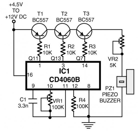
The circuit generates pulses of 1.25 Hz from pin 1 and 20 Hz from pin 14. The three output pins of IC1 are connected to the base terminals of transistors T1, T2, and T3 through resistors R1, R2, and...
Power and serial communications are provided by the FTDI USB to RS232 converter chip. No additional setup is required; simply connect the USB cable from the computer to the board, and a new serial COM port will be installed...
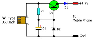
This simple circuit provides a regulated output of 4.7 volts for charging mobile phones. A USB outlet delivers 5 volts DC at a current of 100 mA, which is adequate for slow charging of mobile devices. Most mobile phone...
The clock is constructed using 25 CD4000 integrated circuits (ICs), three 555/556 ICs, and several discrete components. It features an alarm and a method for setting the time that is typically only seen in microcontroller designs. The complexity of...