
Use of N-channel power MOSFET on BQ78PL114

The proposed circuit design aims to optimize the efficiency of the BMS by integrating advanced MOSFET technology and thoughtful component selection. The use of N-channel MOSFETs is particularly advantageous due to their lower on-resistance, which directly translates to reduced power loss and heat generation during operation. The inclusion of a charge pump and a high-voltage ideal diode driver enhances the system's performance by ensuring rapid switching capabilities and reliable operation in high-voltage scenarios.
Furthermore, careful consideration of the current sensing mechanism is essential to maintain the integrity of the battery management system. The integration of current sensing within the MOSFETs can streamline the design, potentially reducing the number of discrete components required and improving overall system reliability.
The voltage management strategy, utilizing a voltage divider, ensures that the driver operates effectively under varying load conditions, while the proposed safeguards against potential issues related to ground lift highlight the attention to detail necessary in high-performance applications.
Overall, this circuit design reflects a sophisticated approach to battery management, emphasizing efficiency, reliability, and performance in ultralight hybrid electric vehicle applications. The careful selection of components and the innovative use of existing technologies position this design as a forward-thinking solution in the field of electric vehicle engineering.I have finally finished my first prototype PCB but I am a bit worried about the amount of heat generated when using the BMSat max power in myapplication (ultralight hybrid electric vehicle). At 30A cont/50A burstI have almost 20Wloss. It seems to me that it would be possible to reduce power consumption to less than half of that without increasing
costsusing: The use of N-channel MOSFETs enables a muchbetter selection of verylow Rds parts. Itwould obviouslyrequire a different driver design, but as far as I can see, there is nofundamental reasons why this should not work It isused on TI battery AFEs like the bq29330. Using MOSFETs with integrated current sensing would again reduce the number for available devices but reduces the power loss ofthe current current (!) sensor.
This would either require low-side switching or current sensing level shifting to be compatible with the BQ78PL114 current sensor inputs. Here is suggested circuit for implementing a charge pump and driver in aSOT23-6 capsule. It requires only a few parts more than the bq78PL116 reference design. The suggestion make use of a new high voltage ideal diode driver from Nat. Semi that handles 75V (100V peak). It works by monitoring voltage on both sides of the FET via the IN and OUT terminal. It will turn on the gate when the IN pin is raised minimum 30 mV higher than OUT pin using a charge pump supplying 30uA gate current.
The gate voltage is then raised until the IN and OUT levels are identical or until the gate voltage is clamped by an internal zener diode. If the IN pin voltage becomes 30 mV less than OUT pin the gate charge will be shorted to drain within 50-100ns using a built-in high current FET.
This is controlled by the voltage divider R1/R4 (R7/R3) that feed OUT with a voltage around half battery voltage when DSC (CHG) is active and around 8V above IN when DSC (CHG) just becomes inactive. I have not tested the circuit yet since the driver IC have just been released. A possible killer could be that the IN or GATE pins get driven high when ground is lifted. That could be fixed by using an additional p-MOSFET to turn on VS when DSC (CHG) signal is active. The best P-MOSFETs for 100V (16S with some margin) I have found have Rds=19mohm. For the same price I get N-MOSFET with Rds of 3. 5mohm. Inclduing the loss in the body diode the P-channel version has almost four times as high loss at 30A requiring extra heat sink.
500uA is probably too much, I would prefer less than 10uA. The worst seems to be max voltage: 16 cells have typical max charge voltage of 67 volt so the driver should handle at least 70 V continously and 100 V peak minimum. Unfortunately N-channel MOSFET drivers suitable for bq78PL116 seems to be scarce if not non-existing as most high side MOSFET drivers that handle voltage above 70V are made for dynamic applications and lack independent charge-pump.
These are the closest alternatives I have been able to find so far: MAX1614 from Maxim has only 25uA max on current and 6uA max off current but is slow (gate current: charge 15-60uA, discharge 0. 5-2 mA) and handles 26V max battery voltage. This should work but is it not odd to discharge the battery unevenly by design The primary purpose of a balancing BMS is to keep the cells balanced, not unbalanced In addition, if the TPS61041 stops for some reason, then the datasheet says that VIN will be connected to SW so an extra transistor should be added to prevent shorting of the uppermost cell voltage as shown in the datasheet.
A peek at app note SLVA136 shows an alternative way where they use another chip to supply 3. 3V to VIN and EN from the same cell. But it all adds up the number of parts. Especially if the system, like mine, do heavy charge and discharge cycles thru the same wire - then the N-channel driver must be duplicated for the CHG signal so the number of required parts more than doubles compared to the LM5050-1 based suggestion (w 🔗 External reference
Related Circuits
The following diagram illustrates a 50W offline switching power supply circuit design. The circuit is powered by a MOSFET, specifically the BUZ80A/IXTP4N8 for a 220V AC voltage input and the GE IRF823 for a 110V AC input voltage. The...
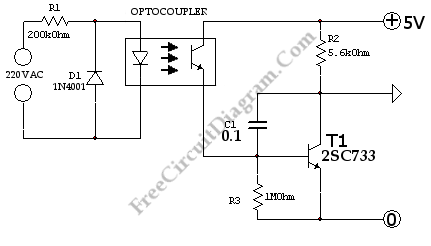
This is a simple 220V power interface circuit. This circuit is used as an interface for monitoring electrical devices and equipment using a computer. The 220V power interface circuit serves as a critical connection point between high-voltage electrical systems and...
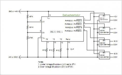
The PS10 saves board space, improves accuracy, eliminates optocouplers or level shifts, and reduces overall component count by combining four programmable timers, input under-voltage (UV) and over-voltage (OV) supervisors, a programmable power-on reset (POR), and four 90V open drain...

A 5V Switch Mode Power Supply utilizing the LM2674 power supply. Refer to the corresponding page for an explanation of the related circuit diagram. The 5V Switch Mode Power Supply (SMPS) designed with the LM2674 integrates a step-down (buck) converter...
.jpg)
Sealed lead-acid batteries are commonly used in power electronics applications, including uninterruptible power supplies (UPS), inverters, and emergency lamps. They provide power to the load when utility power is unavailable. Upon restoration of utility power, a charger supplies power...
The regulator board of the ES301 has been inspected, revealing that the PCB contacts of the current sensing resistors R42 and R43 are severely burned. There is a nearby group of resistors that also need to be replaced, but...