
Vacuum Tube Preamplifier Analysis and SPICE Simulation
The AC model for the triode is an essential tool in understanding the behavior of triode amplifiers in various applications. The equivalent circuit technique allows for simplified analysis and design of amplifiers, facilitating the evaluation of performance metrics such as gain and frequency response. The interplay between AC and DC signals is crucial, as capacitors behave differently under these two conditions, leading to distinct operational characteristics.
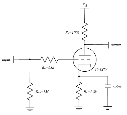
The grid bias resistor plays a significant role in establishing the DC operating point of the triode, ensuring optimal performance by maintaining a stable bias voltage. Similarly, the bypass capacitor allows for effective AC signal processing by isolating the AC component from the DC circuit, thus preserving the integrity of the AC signal. The grid resistor's interaction with parasitic capacitances further shapes the amplifier's frequency response, ensuring that unwanted high-frequency oscillations are mitigated.
The small signal model's parameters, rp and gm, are vital for predicting the amplifier's response to small input signals. By understanding these parameters, designers can optimize amplifier performance, ensuring that the desired gain is achieved while minimizing distortion. The derived gain expression illustrates the relationship between input and output voltages, providing insight into the amplifier's operation.
In conclusion, the AC model for the triode, along with its associated parameters and configurations, serves as a fundamental framework for analyzing and designing triode-based amplifiers. This understanding is crucial for engineers and designers working in the field of electronics, particularly in audio and communication systems.The concept of an AC model for the triode is presented and the equivalent circuit technique is described. Theoretical calculations for amplifier gain and frequency response are derived and compared to simulation results in the SPICE3 environment where good agreement is shown.
The characteristic properties of AC and DC signals are apparent from fun damental circuit theory. As an example, a capacitor behaves as a DC block. However, it will pass AC signals in general, but the transfer will be contigent upon signal frequency, type of capacitor, and total capacitance. Here it should be noted that these differences are attributed to the mechanism of current flow in each case.
DC signals move charge by conduction. Electrons from one part of the circuit travel continuously to another point due to an electric field that is created by a potential difference, or voltage. Once the capacitor is charged up by the conduction of charge to each plate, the capacitor appears as an open circuit to DC signals.
By contrast, AC signals move through capacitors by the mechanism of displacement. Small amounts of charge are moved to and from the plates of the capacitor. They are not conducted through the capacitor. However, this displacement of charge is the means by which AC signals propagate through capacitors. Lastly, it is important to understand that the AC signal is superimposed upon the DC signal and thus the two components obey the mathematical laws of superposition: namely, the AC and DC components can be considered separately and superimposed. However, it should be noted that this is only true to a first order since AC nonlinearities in the tube will give rise to DC components, but this is beyond the scope of this paper.
It is equally important to recognize that the two components are interrelated. This will become apparent shortly. It is important to understand the purpose of each element in the configuration. The grid bias resistor, RGB, provides a high resistance (DC) path to ground and thus it biases the grid to zero volts DC. Moreover, it sets the input resistance into the amplifier. It is generally desirable for the input resistance of an amplifier to be as high as possible so the input signal is not attenuated by the voltage divider set up by the amplifier input resistance and signal source resistance.
The bypass capacitor, CB, provides an AC path from the cathode to ground. Therefore, the cathode resistor, RK, does not influence the AC signal since the cathode is effectively an AC ground. The grid resistor, RG, limits the frequency response of the amplifier by interacting with the capacitance between the grid and plate to create an RC circuit with a -3dB point, or half power point, of about 20kHz as will be shown later.
This will damp any oscillations that may occur at higher frequencies and therefore stablize the amplifier. The plate and cathode resistors simply limit the DC current in the tube, or more specifically, they are what set the bias point.
However, these components will also set the gain as will be shown. Next, it is instructive to define certain AC parameters of the tube so an AC model, more commonly called a small signal model, may be derived. Be aware that the small signal model is exactly that: a model. Models are intended to approximate the real physical operation of a device. The operation of tubes, or any device for that matter, is rather complex and nonlinear in general. However, if one can represent the operation of the device by familiar and simple linear circuit elements, such as resistors and capacitors, then the model may make analysis much easier.
These parameters that are defined below are inherent to the model and bear no real significance except for providing a method for notating the physical properties of the device. The parameters are as follows. Here rp is the dynamic plate resistance, gm is the mutual conductance, and m is the amplifier gain. Do not confuse m with the actual gain of the circuit. This parameter actually quantifies the open loop, or unloaded, gain of the amplifier. Thus m is actually the maximum achieveable gain. For those unfamiliar with calculus, the ¶ operator represents a partial derivative of a multivariable function with respect to the variable in the denominator.
This can be thought of as a differential change or a very small change of one parameter with respect to the other. The straight bar means while holding constant. So in words, the dynamic plate resistance, rp, is a small change in the plate voltage with respect to a small change in the plate current while holding the control grid voltage constant.
Mutual conductance is often misunderstood, but if the definition is simply explained in words as above, it becomes less confusing. The mutual conductance is the change in plate current with respect to grid voltage while holding the plate voltage constant.
What does this mean Well, it is simple. If the grid voltage changes just a little bit, then a small amount of change in the plate current is induced. The ratio of this is the mutual conductance. This is fundamental to tube operation. The control grid controls the current from the plate to cathode. Here we have simply quantified that fact. The role of gm will be apparent in the small signal model. We are now ready to discuss the aforementioned small signal model. The small signal model makes use of these differential parameters. Although there is no absolute definition of what a small signal is, it is safe to assume that the audio signal is always small in preamp circuitry.
A more rigorous definition that holds generally is that a small signal must incur no more than 5% THD, or total harmonic distortion. Please note that power amp stages cannot be modeled by this small signal model since the signal is large and the differential parameters do not apply.
There are some simple rules for determining the small signal equivalent circuit. This is to be done only for analysis by hand and therefore do not actually do this to a circuit. The rules are as follows: Short all coupling and bypass capacitors by virtue of being AC short circuits. Short the power supply to ground by virtue of the low resistance path through the supply rail and the AC decoupling cap to ground.
Replace the active device (tube) with the appropriate small signal model. One may wonder why in this model the capacitors are not short circuits to the AC signal. This is due to the fact that these capacitors do effect the AC signal. They are inherent to the triode and by including them, the model becomes more accurate the frequency response of the device can be determined. The capacitors that were shorted previously were bypass capacitors and thus are typically very large so the AC impedence is very small and thus these capacitors behave as short circuits.
The parasitic capacitors in the model above are are small by comparison and thus the associated impendence is not negligible. Now let`s look at our model for the common cathode using the rules for determining the small signal model.
Fig. 6A shows the midband model, which will be used to determine the gain, while Fig. 6B shows the model with the parasitic capacitors which will be used to find the cut-off, or -3dB, freqeuncy. In both figures, the dependent current source model has been selected since it is easiest to analyze.
However, the dependent voltage source model could also be employed. To find the gain we simply need to find the output current and then combine resistances in parallel. We readily notice from the model how a negative sign will be introduced into the gain equation. This is a function of the control grid`s operation as described previously. Now to perform the analysis. The voltage at the plate, or output, will be the product of the current to the output and the parallel combination of rp and RA. Of course the current to the output is simply gmvg and thus the gain is simply vout/vg. The derivation of the final gain expression is shown below where Av denotes the voltage gain. 🔗 External reference
Related Circuits
There is growing interest in utilizing PC and workstation platforms for reactive sound synthesis and processing applications. However, few operating systems are designed to provide real-time performance, and vendors typically do not guarantee or specify the expected performance levels...
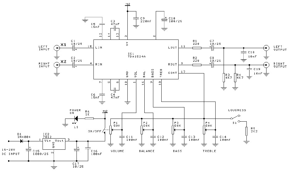
Preamplifier and tone control circuit based on the TDA1524A. The tone control circuit module is included in this preamplifier circuit, allowing for direct connection of the output channels to a stereo power audio amplifier circuit. This RIAA stereo preamplifier...
Design and dimensioning of active low-pass and high-pass filters using Sallen-Key and multiple feedback topologies. Spice netlist generator. Active low-pass and high-pass filters are essential components in signal processing, allowing specific frequency ranges to pass while attenuating others. The Sallen-Key...
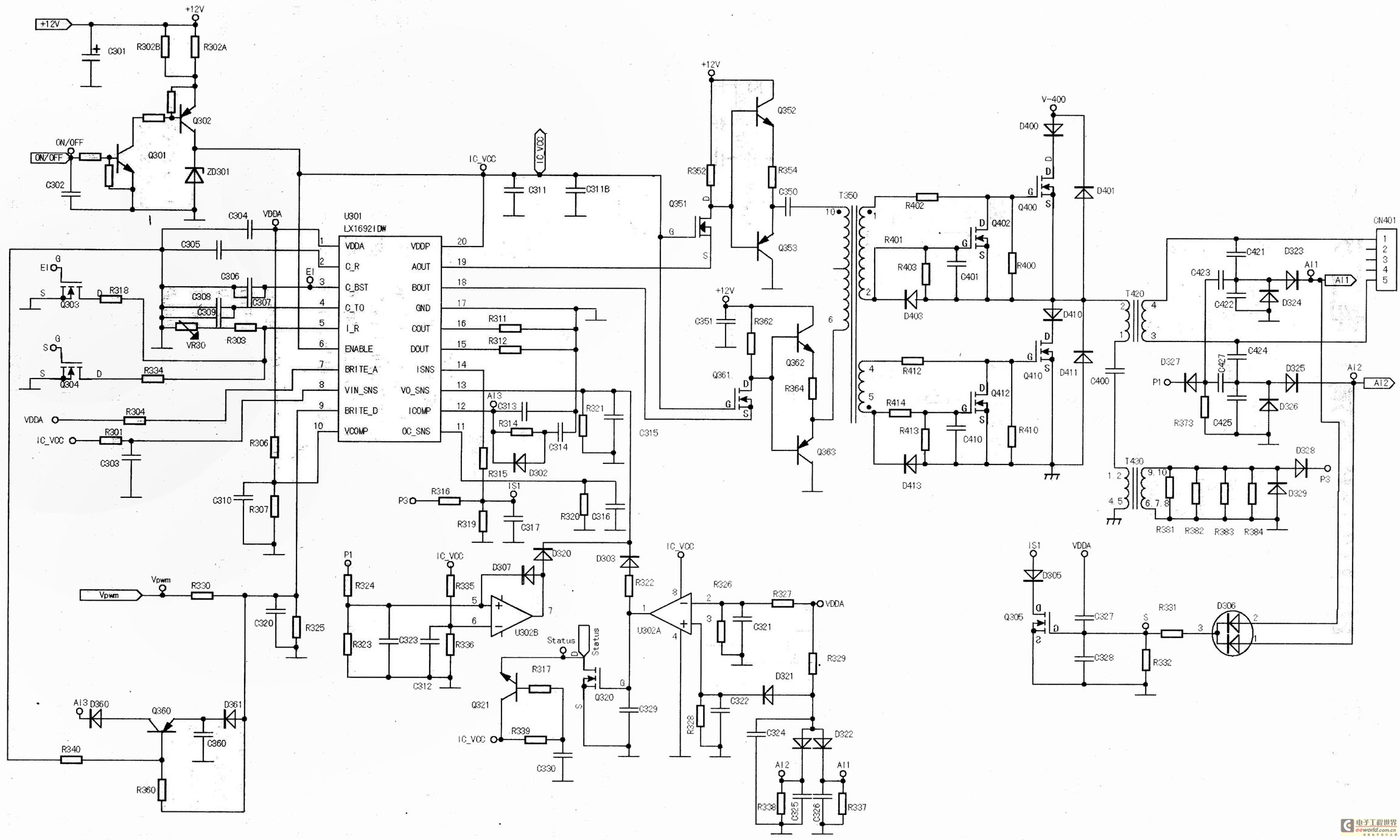
The main component is the LG26 one-inch screens integrated with the FSP107-2PS01 two-in-one electrical power package, which utilizes a direct drive CCFL modulator tube. This setup is compatible with screens from other manufacturers, such as Samsung and AU, but...
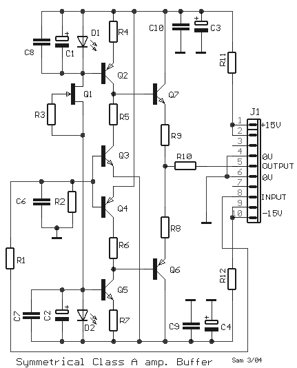
The circuit was designed to create a modular Class A buffer preamplifier to isolate stages in an audio circuit. BF245 is a general-purpose N-Channel JFET used in this design. The modular Class A buffer preamplifier serves as an essential component...
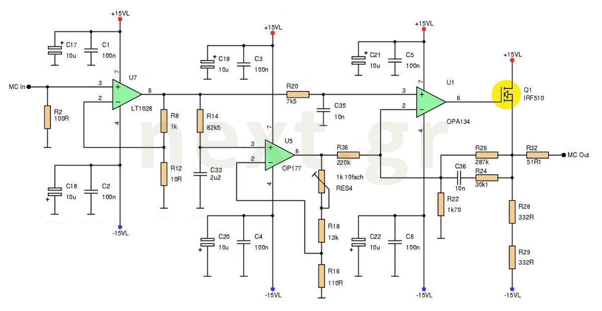
This microphone preamplifier circuit enhances the acoustic signal of a moving coil microphone (MC) with a sensitivity of 150μV at line level. In this design, a specific technique is not employed because the noise produced does not significantly impact...