
Video Amplifier Circuit

The video amplifier circuit is designed to enhance the quality of video signals by amplifying the input signal while maintaining fidelity. The core components include transistors, resistors, and potentiometers that control various aspects of the signal. The transistors, typically configured in a common emitter arrangement, serve as the primary amplification stage.
In this design, the potentiometers P1 and P2 are used to adjust the black level and signal amplitude, respectively. However, extreme adjustments can lead to excessive base current flowing into transistor T1, resulting in thermal runaway or permanent damage. To prevent this scenario, the addition of resistors R3 and R4 is critical. These resistors limit the current flowing into the base of T1, ensuring it remains within safe operating limits regardless of the potentiometer settings.
When the potentiometers are adjusted to their extremes, the resistors effectively create a voltage divider that reduces the base current to T1. This design consideration not only protects the transistor but also enhances the overall reliability of the amplifier circuit.
For optimal performance, the values of R3 and R4 should be carefully selected based on the specifications of the transistors used and the desired range of adjustment for the potentiometers. This ensures that the video amplifier can operate effectively across its entire range without risking damage to its components.
In conclusion, while the basic design of the video amplifier is straightforward, the inclusion of protective components such as resistors is vital for safeguarding sensitive elements like transistors from excessive current and ensuring the longevity and reliability of the circuit.The video amplifier in the diagram is a well-known design. Simple, yet very useful, were it not for the ease with which the transistors can be damaged if the potentiometers (black level and signal amplitude) are in their extreme position. Fortunately, this can be obviated by the addition of two resistors. If in the diagram R3 and R4 were direct co nnections, as in the original design, and P1 were fully clockwise and P2 fully anticlockwise, such a large base current would flow through T1 that this transistor would give up the ghost. 🔗 External reference
Related Circuits

This component is useful for ensuring that the subwoofer is in phase with the speakers of the existing car radio. It utilizes dual-linear motion potentiometers, capacitors, and electrolytic components. The circuit described involves a phase alignment system designed to optimize...
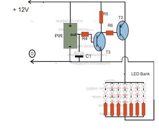
The circuit is an LED driver that responds to ambient light as well as the presence of an intruder, varying its illumination accordingly. Additionally, it includes an ambient light sensor to turn the LEDs on and off, and a...
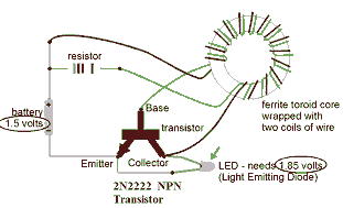
This circuit is known as the Joule Thief. For those unfamiliar with it, an image of the circuit is provided. The Joule Thief is a minimalist circuit designed to extract usable voltage from a low-voltage power source, such as a...
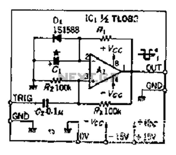
Although people believe that using a timer with an operational amplifier (op-amp) does not yield significant results, it can still be advantageous in certain scenarios. In environments with high noise levels, the application retains its benefits. When the phase...

This alarm system utilizes a loud police siren to deter potential intruders. Activated by a single clap, the circuit triggers the alarm for three minutes, which is adequate to alert nearby residents. The design incorporates a sensitive clap switch...
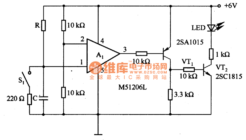
The circuit is designed to set a delay time based on the voltage Us and the resistor R. In this configuration, S1 acts as the discharge switch for capacitor C. When switch S1 is closed, the stored charge in...