
Voltage-Controlled Amplifier
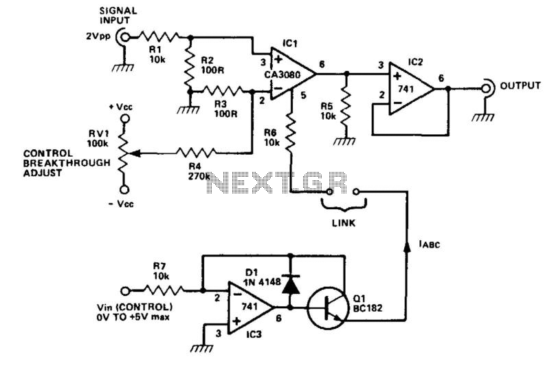
The CA3080 operational amplifier is designed for applications requiring variable gain control. In this configuration, the resistors R1 and R2 form a voltage divider that sets the input signal level to a manageable 20 mV peak-to-peak, ensuring that the amplifier operates within its linear region and avoids distortion. When the input signal exceeds this level, the output may exhibit nonlinear characteristics, which can be beneficial in specific applications like waveform shaping.
The gain control is achieved through the IABC current, which is injected into pin 5 of the CA3080. The relationship between IABC and the gain is critical; as IABC increases from 0.1 mA to 1 mA, the gain increases linearly, allowing for precise control over the output signal. This feature is particularly useful in applications where dynamic range and signal integrity are paramount.
The output of the CA3080 is a current that must be converted to a voltage for practical use. This is accomplished by connecting the output to a resistive load, R5, which converts the current output to a voltage output according to Ohm's law (V = IR). The output impedance at pin 6 is specified at 10 kΩ, which can lead to loading effects if not properly managed. To mitigate this, a voltage follower (IC2) is employed to provide a low output impedance, ensuring that the subsequent stages of the circuit receive a stable voltage without being affected by variations in load.
The precision voltage-to-current converter circuit around IC3 plays a crucial role in generating the IABC current. This converter allows for fine adjustments to the gain by varying the control voltage Vm. A positive Vm results in a proportional increase in IABC, thereby increasing the gain, while a negative Vm effectively reduces IABC to zero, disabling the gain altogether. This dual functionality enables versatile applications in signal processing, where both amplification and attenuation may be required. Overall, the CA3080's design and capabilities make it an effective component for analog signal manipulation in various electronic circuits. The CA3080 can be used as a gain controlling device. The input signal is attenuated by R1/R2 so that a 20-mVpp signal is applied to the input terminals. If this voltage is much larger, significant distortion will occur at the output. In fact, this distortion is put to good use in the triangle-to-sine wave converter. The gain of the circuit is controlled by the magnitude of the current IABC. This current flows into the CA3080 at pin 5, which is held at one diode voltage drop above the - VCc rail· The gain of the CA3080 is " "linearly" proportional to the magnitude of the IABC current over a range of 0.1 to 1 mA. Thus, by controlling IABC, you can control the signal level at the output. The output is a current output, which has to be "dumped" into a resistive load (R5) to produce a voltage output.
The output impedance at IC1 pin 6 is 10 kfi (R5), but this is "unloaded" by the voltage follower (IC2) to produce a low output impedance. The circuit around IC3 is a precision voltage-to-current converter and this can be used to generate IABC.
When Vm (control) is positive, it linearly controls the gain of the circuit. When it is negative, IABC is zero and so the gain is zero. 🔗 External reference
Related Circuits
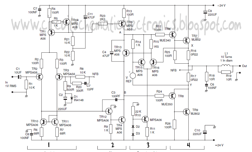
This design schematic represents a Class A power amplifier. It closely matches the operating parameters of Class B to facilitate comparison, particularly with a negative feedback (NFB) factor of 30dB at 20 kHz. The front end is similar to...
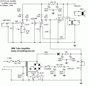
The following diagram represents a 20W power amplifier circuit constructed using the EL34 tube component. The EL34 is a well-known tube that is highly regarded for use in power tube amplifiers. The circuit includes both the tube amplifier schematic...
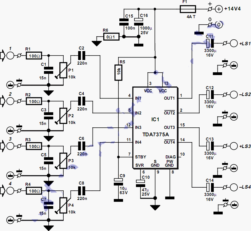
This quad amplifier is designed primarily for automotive use but can also be applied in various medium-power scenarios. The TDA7375A is suitable for situations requiring a reasonable amount of audio power with a relatively low supply voltage. It is...
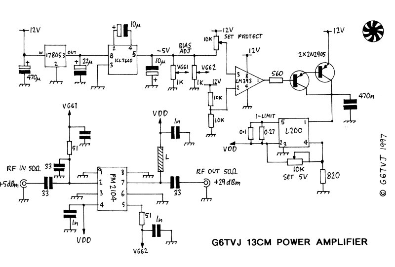
A simple synthesized 13 cm ATV exciter has led to considerations for an appropriate power amplifier. The exciter generates approximately 10 mW, which may be sufficient to drive a MMIC or hybrid amplifier. However, at 2.3 GHz and higher...
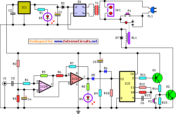
This circuit deactivates an amplifier or any connected device when a low-level audio signal at its input is absent for at least 15 minutes. By pressing P1, the device is powered on, supplying power to any appliance connected to...
This is an RF Power Amplifier designed for low-cost QRP applications. The circuit operates over a broadband frequency range of 1.8 to 30 MHz, eliminating the need for tuning. The only adjustment required is to set the quiescent current...