
Voltage-controlled cipher scheme of constant-current source of output high-power of bipolar
The described circuit utilizes an operational amplifier to create a constant current source, which is essential for various applications requiring stable current delivery. The design's simplicity and cost-effectiveness make it suitable for integration into larger systems, where reliable performance is crucial. The feedback mechanism ensures that any variations in output current are corrected in real-time, maintaining the desired operational parameters. The use of standard components, such as the 78 and 79 series regulators, further enhances the design's accessibility and reliability. The implementation of a difference amplifier allows for precise voltage comparisons, ensuring that the output remains consistent with the intended specifications. Overall, this design represents a robust solution for generating stable output currents in electronic circuits.The output current range of the parameter current regulator is little, the current regulator is not tall in precision; It is small to connect the feedback adjustment type output current of the current stabilized power source in series, efficiency is lower; The steady stream source of the switch not only the circuit is complicated, the components and parts are in large quantity, but also it is great, with discrepancy reliability to output the ripple. In view of the above-mentioned shortcomings, originally design adopting ordinary operational amplifier, cooperate with the triode to expand the voltage and the electric current is expanded, having already achieved the goal of offering the big output current, and the circuit is simple in construction, the cost is lower, precision great. Fig. 1 is a functional block diagram originally designed, are input into the constant current module that the Operational Amplifier forms by the external control voltage signal.
The electric current outputted offers to load after the voltage expands the module and electric current and expands the module. The electric current samples the electric current through sampling the resistance, the acquired sampling signal is feedbacked in the module of constant current to carry on constant current via the feedback system module of voltage.
Among them is expanded the module and electric current to expand the module and supply power by the voltage of pair of module of the power. Choose the on the market commonly used switching power supply to expand the module and offer the output power to the electric current, with the interference elimination in the electric capacity of joining-up in parallel of its Ausgang.
Because of requiring the bipolar output, can save the cost and reduce the volume to choose the switching power supply of bipolar output. In the experiment, it is 1% of the switching power supplies that we use the nominal ripple. Use 78, 79 serial three terminal regulators to offer the voltage to expand the module in order to improve the output voltage of operational amplifier after stepping down.
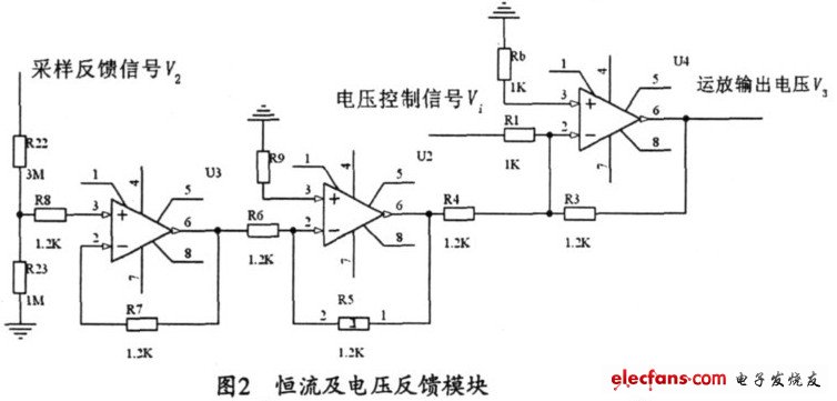
Fig. 2 is constant current module and voltage feedback module of operational amplifier. Since Fig. if you can`t can see since electric current Ausgang 2, gather to sample feedback signal after not dealing with for partial pressure via follower that operational amplifier make up and behind revisor, sent to reverse end and voltage control signal of the reverse adder U4 and add the output voltage V3. V3 formula which is received operational amplifier: It is that the voltage expand the circuit diagram of the module that Fig.
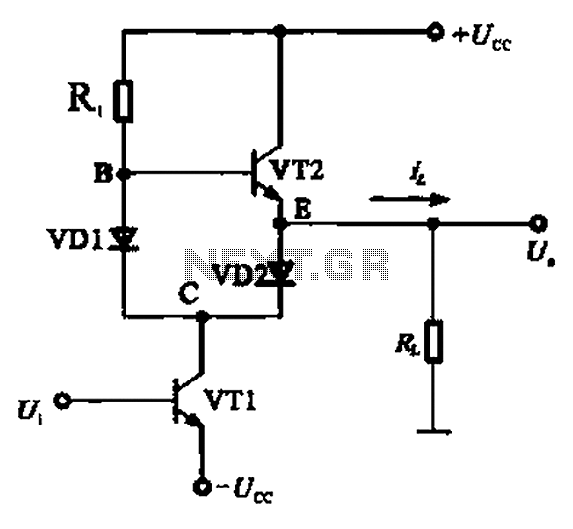
3 shows. Formed the difference amplifier by operational amplifier, compare the signal of system generation of constant current with output voltage with treated partial pressure and amplify, form the final output voltage. The triode in the system chooses the geminate transistor, in order to achieve the purpose of bipolar output, magnification of this systematic open loop is only decided by the ratio of R17 to R14, but after R25 and R24 partial pressure is feedbacked, it is equivalent to the amplifier, its magnification is decided by the ratio of R25 to R24.
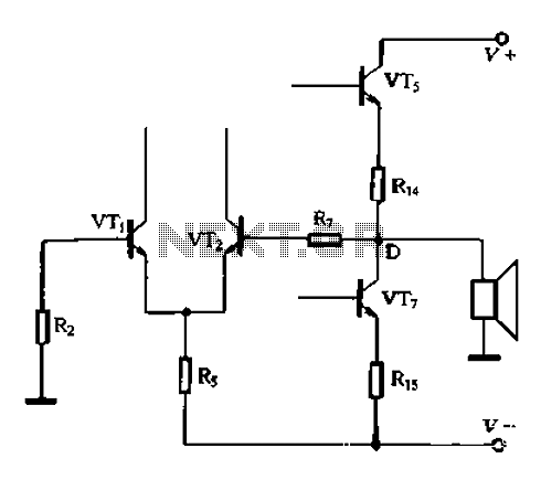
Fig. 4 shows as the expansion circuit of the electric current. The commonly used totem sliding pillar type electric current simple to use expands the method, pay attention to the choice of the power triode, and add the air-cooling fin and guarantee the output power. In this w 🔗 External reference
Related Circuits
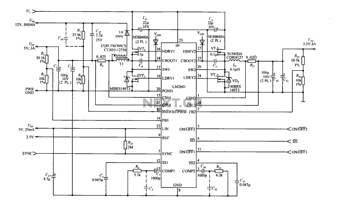
The circuit consists of the LM2641, which provides four output voltages: 5V at 3A, 3.3V at 4A, 12V at 0.3A, and 5V at 0.025A. The LM2641 is a dual adjustable step-down switching power supply controller with an input voltage...
A Class AB output stage circuit is coupled with diodes, as illustrated in Figure 10-8. The static bias circuit for transistor VT1 (not shown) is adjusted so that the output at point E is at ground DC voltage UE....
A, B, and C represent indirect person capacitance. The new access capacitor C is known as the bootstrap capacitor. The self-bootstrap capacitor can increase the voltage at point A. When static, Vi = 0V, the midpoint voltage VD is...
This circuit sequentially lights ten bulbs, first in one direction and then in the opposite direction, creating an appealing visual effect. Gates N1 and N2 form an oscillator, which serves as a clock for the BCD up/down counter CD4510...
The circuit is a high-power car audio amplifier schematic. It functions as a car audio amplifier using the PA02 and LH0101 integrated circuits (ICs). Each IC delivers an output power of 30W with an 8-ohm impedance. The part list...
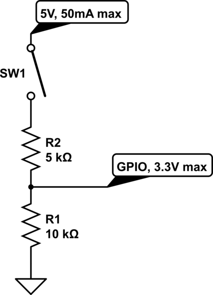
The circuit is designed to limit the maximum voltage between the GPIO input pin and the current source to 3.3V. This is achieved through a voltage divider configuration where the voltage across the 10K resistor is 3.3V, while the...