
Voltage Doubler and InverterCircuit with Schematic
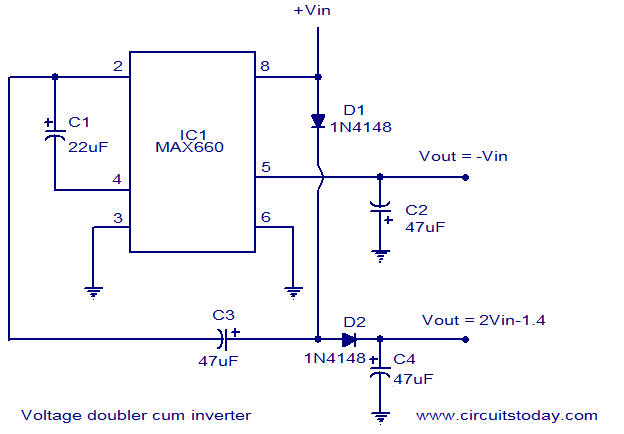
The MAX660 integrated circuit (IC) is designed for applications requiring a voltage multiplier, specifically functioning as both a voltage doubler and inverter. The circuit utilizes the MAX660 to convert a low input voltage into a higher output voltage, effectively doubling the input voltage while also allowing for inversion of the polarity.
In the voltage doubler configuration, the MAX660 operates by charging capacitors during alternating cycles, which leads to the accumulation of charge and results in a doubled output voltage. The circuit typically includes input and output capacitors, which smooth the voltage output and minimize ripple. The input voltage is applied to the circuit, and through a series of switching actions managed by the IC, the output voltage is generated.
For the voltage inverter operation, the MAX660 is configured to produce a negative output voltage. This is achieved by utilizing the same principles of charge accumulation and capacitor switching, but with the output stage designed to invert the voltage polarity. The inverter circuit is particularly useful in applications requiring a negative supply voltage, such as operational amplifiers or other analog components that necessitate dual supply voltages.
The schematic for both configurations will include the MAX660, input and output capacitors, and potentially additional components such as resistors or diodes to ensure proper operation and stability. The output characteristics can be influenced by the choice of capacitors and the load connected to the output, which should be considered during circuit design to achieve desired performance specifications.
Overall, the MAX660 provides a compact and efficient solution for generating higher voltages and negative voltages from a low-voltage DC source, making it suitable for various electronic applications.Voltage Doubler circuit and Voltage Inverter circuit diagram with schematics using MAX660 IC -which is a DC voltage multiplier IC. This is a dc voltage doubler circuit and inverter.. 🔗 External reference
Related Circuits
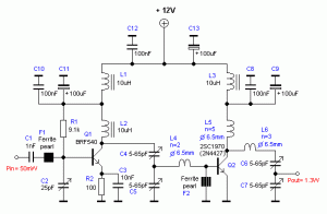
The RF power amplifier circuit described here utilizes the transistors 2SC1970 and 2N4427. This FM RF amplifier operates within the frequency range of 88-108 MHz, delivering an output power of approximately 1.3W from an input driver of 30-50mW. The...
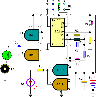
This circuit is designed to provide alerts after a predetermined time interval. It is ideal for tabletop games that necessitate a fixed duration for answering questions or moving pieces. In this context, it serves as a contemporary alternative to...
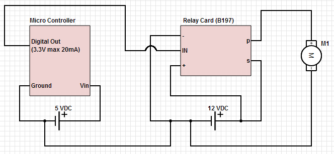
The objective is to control a 12 VDC device (on/off) from a microcontroller using a relay card. The relay requires a 12 VDC operating power supply. To achieve the control of a 12 VDC device using a microcontroller and a...
Two low voltage, low power zeners are used to control electronically the level of an audio signal. The attenuation range is from 6 to 58dB for an input current from 0.042 to 77mA corresponding to a control voltage from...
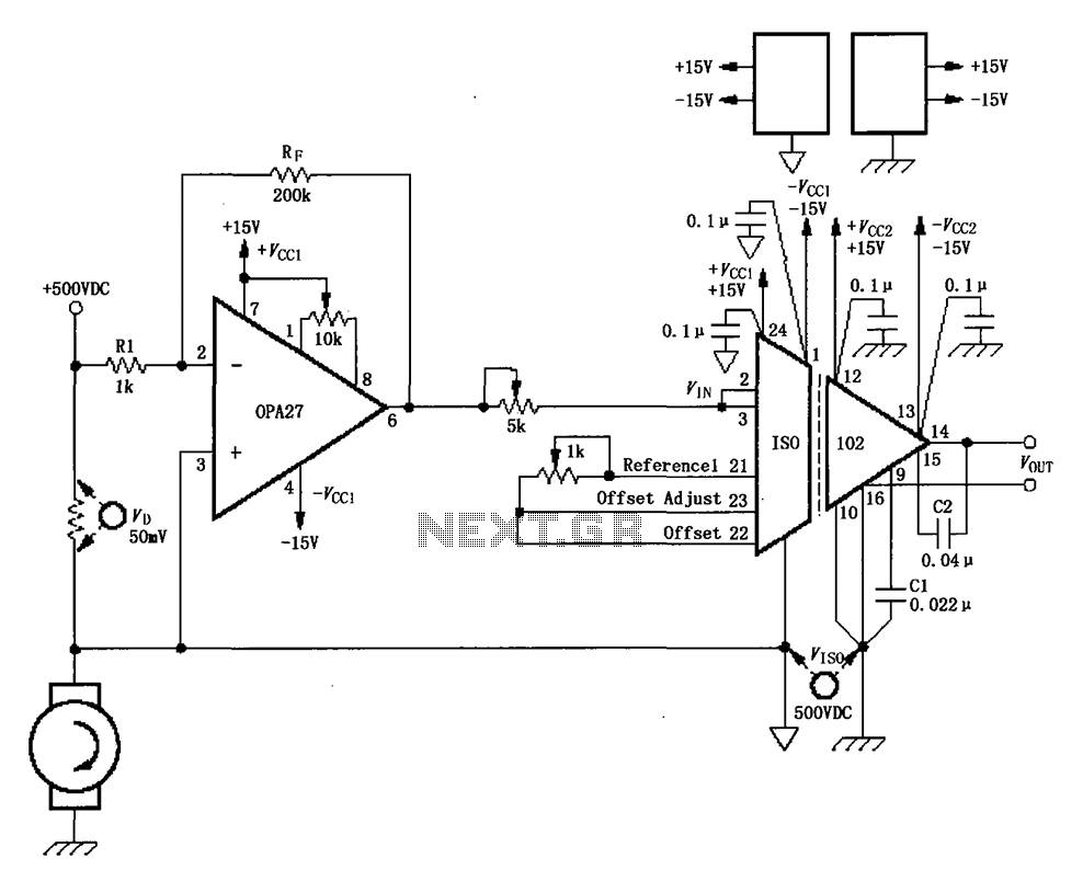
The circuit depicted in the figure consists of an ISO102 and OPA27 for measuring DC current at a voltage of +500V. It is configured between a +500V DC voltage source and a sampling resistor that is in series with...
Circuit CREATOR Electronics CAE System provides the most complete and high performance solution for electronics design using personal computers. More: Includes PCB DESIGN -layout editor and Schematic Capture software tool, full Schematic Design and Capture, Circuit Simulation, full interactive...