
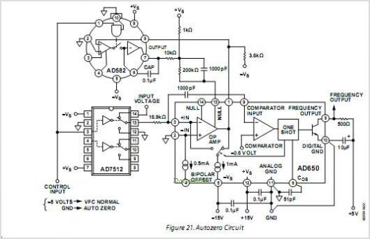
Voltage-to-Frequency And Frequency-to-Voltage Converter
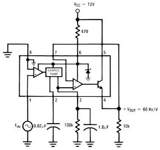
The AD652 Synchronous Voltage-to-Frequency Converter is a highly versatile device utilized in applications requiring precise analog-to-digital conversion. The device's architecture is based on a synchronous operation that ensures low nonlinearity, making it suitable for high-accuracy applications. The typical nonlinearity of 0.002% ensures that the output frequency remains consistent with the input voltage across a wide range of conditions, which is critical in systems where precision is paramount.
The use of an external clock to define the full-scale output frequency is a key feature of the AD652. This design choice enhances stability and linearity, as it decouples the conversion process from the inherent variability of external capacitors. This feature is particularly beneficial in environments where temperature fluctuations and component aging could otherwise affect performance.
Gain drift is a critical parameter in precision applications; thus, the AD652 incorporates a low-drift reference and low TC thin-film scaling resistors on-chip. This design minimizes variations in gain over temperature and time, ensuring consistent performance. The implementation of laser-wafer-trimming to reduce initial gain error to below 0.5% further enhances the device's reliability and accuracy.
The operational flexibility of the AD652 is enhanced by its capability to function from a single-ended power source, which simplifies its integration into various systems. This feature is particularly useful in isolated power supply scenarios, where minimizing complexity is essential.
The AD652's availability in multiple performance grades allows for selection based on specific application requirements, including temperature range and packaging type. The 20-pin PLCC and 16-pin cerdip package options provide flexibility in design, catering to both commercial and industrial applications. The extended temperature range variant (AD652SQ) is particularly advantageous for applications in extreme environments, ensuring reliability and performance across a broad spectrum of operating conditions. Overall, the AD652 is an essential component for engineers seeking high precision in analog-to-digital conversion tasks.The AD652 Synchronous Voltage-to-Frequency Converter (SVFC) is a powerful building block for precision Analog-to-digital conversion, offering typical nonlinearity of 0. 002% (0. 005% maximum) at a 100 kHz output frequency. The inherent monotonicity of the transfer function and wide range of Clock frequencies allows the conversion time and resolution
to be optimized for specific applications. The AD652 uses a variation of the popular charge-balancing technique to perform the conversion function. The AD652 uses an external Clock to define the full-scale output frequency, rather than relying on the stability of an external capacitor.
The result is a more stable, more linear transfer function, with significant application benefits in both single and multichannel systems. Gain drift is minimized using a precision low drift reference and low TC on-chip thin-film scaling resistors.
Furthermore, the initial gain error is reduced to less than 0. 5% by the use of laser-wafer-trimming. The Analog and digital sections of the AD652 have been designed to allow operation from a single-ended power source, simplifying its use with isolated power supplies. The AD652 is available in five performance grades. The 20-pin PLCC packaged JP and KP grades are specified for operation over the 0C to +70C commercial temperature range.
The 16- pin cerdip-packaged AQ and BQ grades are specified for operation over the -40C to +85C industrial temperature range, and the AD652SQ is available for operation over the full -55C to +125C extended temperature range. 🔗 External reference
Related Circuits
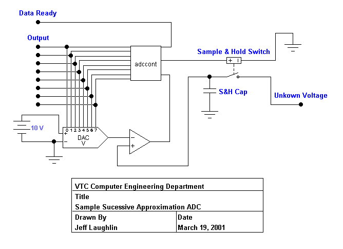
The successive approximation Analog to Digital Converter (ADC) is one of the most common types of ADC. It requires few components and is straightforward to operate. Additionally, it always takes the same amount of time to calculate the result....
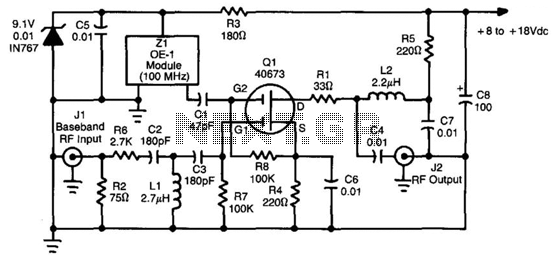
This converter utilizes a 40673 MOSFET to heterodyne the 5.5 to 8 MHz TVRO subcarriers to the FM broadcast band, enabling the use of a stereo receiver for high-fidelity stereo reception of TV sound subcarriers. Z1 is a prepackaged...
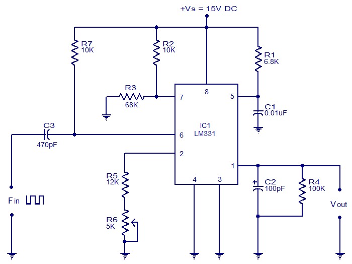
The following circuit illustrates a Frequency Voltage Converter Circuit. This circuit is based on the LM331 IC and operates with a supply voltage of 15V DC. The Frequency Voltage Converter Circuit utilizes the LM331 integrated circuit, which is designed for...
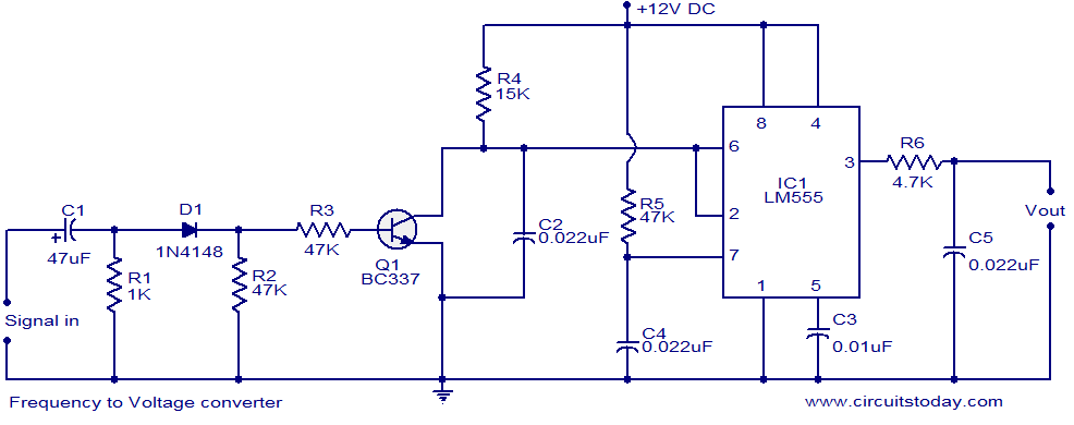
A simple frequency to voltage (F to V) converter circuit utilizing the LM555 Timer IC. This circuit has numerous applications in digital frequency meters, tachometers, and other related devices. The frequency to voltage (F to V) converter is a crucial...
The LM2917 IC chip is specifically designed as a Frequency to Voltage Converter. It requires only a few external components for its operation. The datasheet for the LM2917 IC includes several application examples of the Frequency to Voltage Converter....
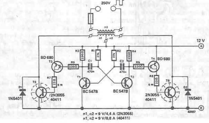
A simple portable converter that transforms 12V to 250V can be constructed using this circuit diagram. This converter is intended for portable use with a 12V car battery. A built astable multivibrator, consisting of transistors T1 and T2, generates...