
Waging the War on Power in 3G Mobiles
The design of a 3G mobile device circuit must account for the integration of various components to ensure optimal performance and power efficiency. A single-chip architecture is preferred for its ability to minimize inter-processor communication overhead, which can significantly drain battery life. The integration of baseband processing and application processing on a single chip allows for direct communication between the cores, reducing latency and enhancing overall system performance.
The architecture may include a combination of analog and digital components, such as a digital signal processor (DSP) for handling complex algorithms, a baseband processor for processing the radio signals, and an application processor for managing user interface and application tasks. The use of an L1 cache within the architecture facilitates faster data access, thereby improving the processing speed when interfacing with slower external memory systems.
Furthermore, the design should implement power management techniques, such as dynamic voltage and frequency scaling (DVFS), to adjust the power consumption based on the workload dynamically. This can be achieved through dedicated hardware that monitors system performance and adjusts clock rates and voltage levels accordingly, thus optimizing power usage.
To enhance the flexibility of the system, a programmable core may be included for tasks that require frequent updates or changes. This hybrid approach allows for the rapid deployment of new features while maintaining the efficiency of hardware accelerators for performance-critical tasks.
In summary, the circuit design for a 3G mobile device must prioritize a single-chip architecture that integrates baseband and application processing, employs efficient memory management, and utilizes intelligent hardware/software partitioning to achieve a balance between performance and power consumption, ultimately extending battery life and enhancing user experience.Consumers of mobile wireless devices expect a workable, real-world balance of performance and battery life. This is particularly applicable in third-generation (3G) wireless designs, due to the fact that these devices will house more powerful and feature rich multimedia capabilities.
With processor performance (Moore`s law) doubling every 18 month s and communications system performance (Shannon`s Law) doubling every 8. 5 months, battery energy density has not kept up —it doubles every ten years. This highlights a significant technology gap. To bridge this supply/demand power gap, system engineers need to implement an arsenal of technologies ranging from process, software, and circuit innovations to meet the power requirements of 3G phones. Let`s look at some of the tools in this arsenal in more detail. To meet the demands of 3G mobiles, many OEMs are looking at a dual- or triple-processor architecture to handle baseband processing tasks.
However, when examining architectures, a single chip, which combines cores for baseband and application processing, has obvious advantages over multi-processor designs. Having separate and independent processing resources requires a sophisticated inter-processor communication network to perform data exchange and control.
The complexity of this approach increases with each processor added to a baseband design. Thus, inter-processor communication can become a formidable design challenge to software and hardware designers. The complexity of inter-processor communication networking overhead reduces the processing performance available for end-user applications and increases power consumption, which results in reduced battery life and usage time for the end user.
In addition, monitoring for the presence of wireless networks requires interaction between the application processors for each connectivity node to be monitored (WWAN, WLAN, GPS, WPAN). This periodic activity and the complexity associated with inter-processor communication introduces additional processing overhead that consumes battery power.
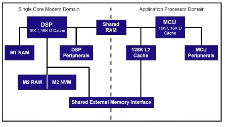
By employing a single chip architecture, the inherent reduction of power consumption is obtained by utilizing fewer processing cores (one core for the modem and one for the applications) and keeping the communications on-chip between the remaining two cores. In addition, providing on-chip memory mirroring reduces the number of external accesses to a minimum resulting in improved battery life (Figure 1).
The single-chip modem architecture shown in Figure 1 incorporates an L1 cache improving performance when using slower memory systems. It also provides additional power savings by reducing the frequency of accesses to the external memory system.
Many tasks in an embedded system can be implemented in either dedicated hardware or in software on a programmable core. Generally, software is more flexible and cheaper, but hardware is faster and consumes less current. The challenge is partitioning tasks between hardware and software to take best advantage of its attributes to get the fastest yet most efficient solution.
A better model for speed and efficiency can be realized by committing intensive machine cycling tasks to hardware accelerators rather than software. However, this must be accomplished in a manner that preserves the flexibility of software where that flexibility is most important.
Functions that are less well defined and can change frequently increase the need for software flexibility over the benefits of dedicated hardware. Intelligent hardware/software partitioning decisions of this sort accomplish a great deal toward high performance, low power results.
An effective method of power optimization is the reduction of transistor switching activity. Architecture partitioning with respect to transistor switching activity allows disabling the clock signals or reducing the clock rate in certain regions of the ASIC, depending on the syste 🔗 External reference
Related Circuits
This circuit is not entirely new, but it is straightforward, dependable, robust, and short-proof. It offers variable voltage up to 24V and adjustable current limiting up to 2A. Customization to meet specific requirements is possible, as detailed in the...
The mechanical and electrical schematic in Figure 5 illustrates a simple circuit comprising several components. The first component is an electronic crossover section utilizing the NE5532 operational amplifier, which is known as the "Emperor of the op-amp." This section...
The expansion board had six servo ports, but the cost did not justify the number of ports. A modification was made to the handyboard, allowing for a total of 16 servo ports at a minimal cost of approximately $2,...
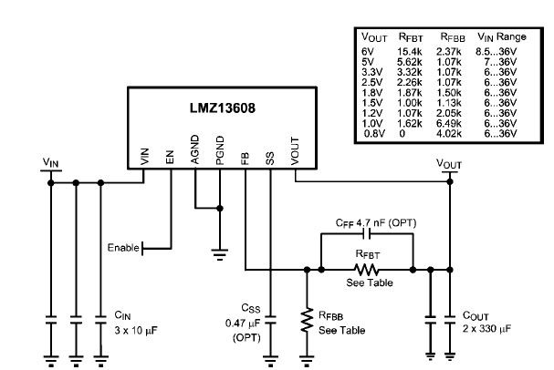
A simple, high-efficiency switching power supply circuit can be designed using the LMZ13608 8A regulator. This regulator offers very high efficiency and requires few external components. It supports a wide input voltage range of 6 to 36 volts and...
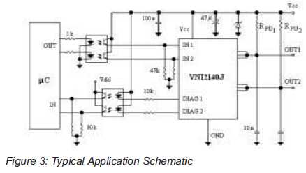
An integrated solution for two output channels that simplifies design and enhances reliability. The device, the VNI2140J, integrates on-chip two 45V Power MOSFET channels with a typical Rds(on) of 80mOhm at 25 degrees Celsius. The VNI2140J is a highly integrated...
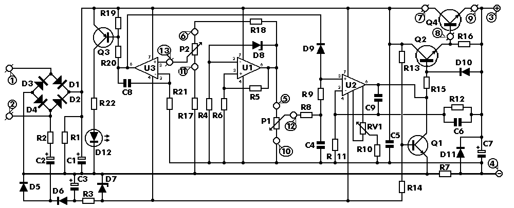
The circuit safely delivers approximately 20 Amps at 13.8V. For lower current applications, a separate current limiting output capable of 15mA up to a total of 20A has been included. The power transformer should be able to supply at...