
wave antenna circuit

The antenna amplifier circuit utilizes two transistors, the BF256C and BF494, which are well-regarded for their performance in RF applications. The BF256C serves as the input stage, providing initial signal amplification and buffering to isolate the input from subsequent stages, thus minimizing loading effects. The BF494 is configured in a common-ground arrangement, which effectively increases the overall gain of the circuit while maintaining stability across the specified frequency range.
The design incorporates an inductor, L1, which plays a critical role in tuning the circuit to the desired frequency. The choice of the Amidon core T-37-6 is significant, as it is designed to provide optimal magnetic properties for RF applications. The winding configuration, with 2 turns on the primary and 12 turns on the secondary, is tailored to achieve the desired inductance value for the specified frequency range. Adjustments to the number of turns can be made to accommodate different frequency bands, allowing for versatile applications of the circuit.
Capacitor C1 is essential for tuning the input circuit, allowing the user to adjust the resonance of the circuit to match the frequency of the desired station. The broad response characteristic of the tuned circuit ensures that slight variations in tuning do not significantly impact performance, making it user-friendly in practical applications.
Powering the circuit with a well-decoupled mains supply converter ensures that noise from the power source does not interfere with the amplifier's performance. The output voltage range of 9-12 V is suitable for the transistors used, and the current draw of approximately 5 mA indicates efficient operation. Overall, this circuit exemplifies the integration of traditional components in creating a reliable and effective antenna amplifier for short-wave applications.The circuit presented here illustrates the fact that in spite of all kinds of new component and technology, it is still possible to design useful, and interesting, circuits. The circuit is based on two well-established transistors, a Type BF256C and a BF494. In conjunction with the requisite resistors and capacitors, these form a well-working ante nna amplifier. Note that they are direct coupled. Transistor T1 is the input amplifier cum buffer, while the BF494, in a common-ground configuration, provides the necessary amplification. The amplifier is designed for operation at frequencies between 10 MHz and 30 MHz, which is the larger part of the short-wave range, and has a gain of 20 dB.
Inductor L1 is wound on an Amidon core Type T-37-6. The primary consists of 2 turns, and the secondary of 12 turns 0. 3 mm dia. enameled copper wire. The number of turns may be experimented with for other frequency ranges. The input circuit is tuned to the wanted station with capacitor C1. The response of the tuned circuit is fairly broad, so that correct tuning is easy. The circuit is powered by a well-decoupled mains supply converter that has an output of 9 12 V. The circuit draws a current of about 5mA. 🔗 External reference
Related Circuits
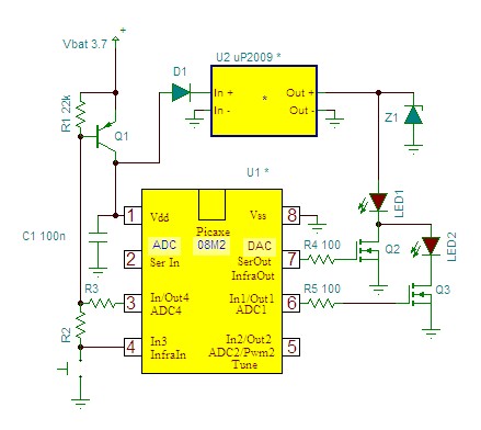
CocaCola clearly stated that his circuit did not work correctly; the series was only complete when both LEDs were enabled, not otherwise. The circuit in question appears to involve a series configuration of light-emitting diodes (LEDs) that require both components...
The circuit configuration for data signal output is designed to optimize transmission distance. It includes an output terminal connected to a pull-up resistor at the receiving end, which works in conjunction with two pull-up and pull-down resistors. The described circuit...

This simple frequency converter mixes the 15-MHz WWV/WVH signal with a 16-MHz signal from the local oscillator (LO) to convert it down to 1 MHz, enabling it to be received on an AM-band receiver. The frequency converter operates by utilizing...
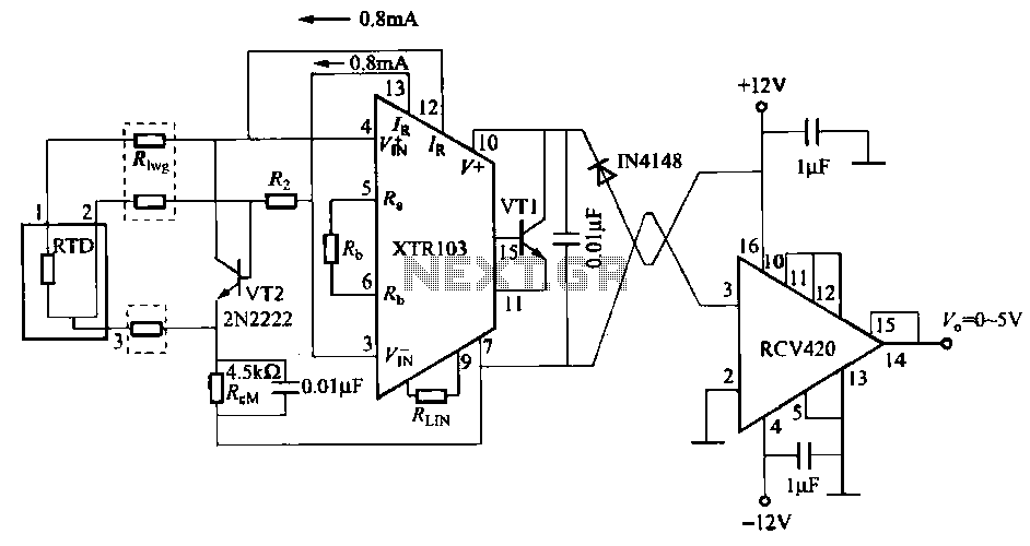
When the RTD temperature sensor is positioned far from the amplifier, the resistance of the sensor leads and their susceptibility to interference and other issues cannot be overlooked. The circuit shown in the figure addresses this problem. It utilizes...
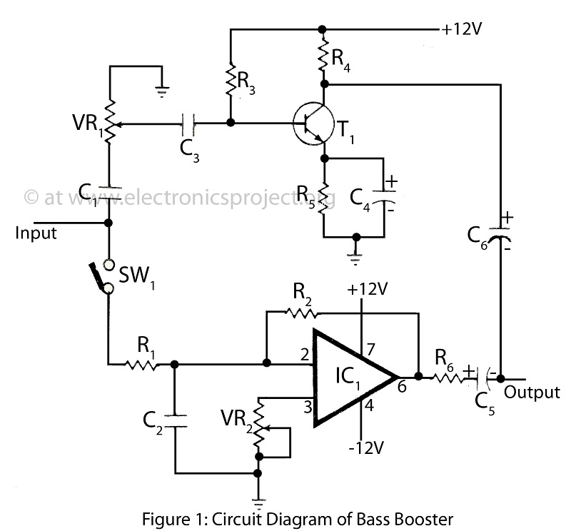
The bass booster featured on this website enhances the beat frequency while maintaining the integrity of the high-frequency response. The circuit diagram for the bass booster, along with various radio circuits, is also provided. The bass booster circuit operates by...
The circuit utilizes the configuration illustrated in Figure 1-36, with the feedback circuit and bias circuit implemented separately. The feedback resistor, Rfl, is approximately 30 ohms. To maintain the desired amplification, the resistor R queue is set to 1...