
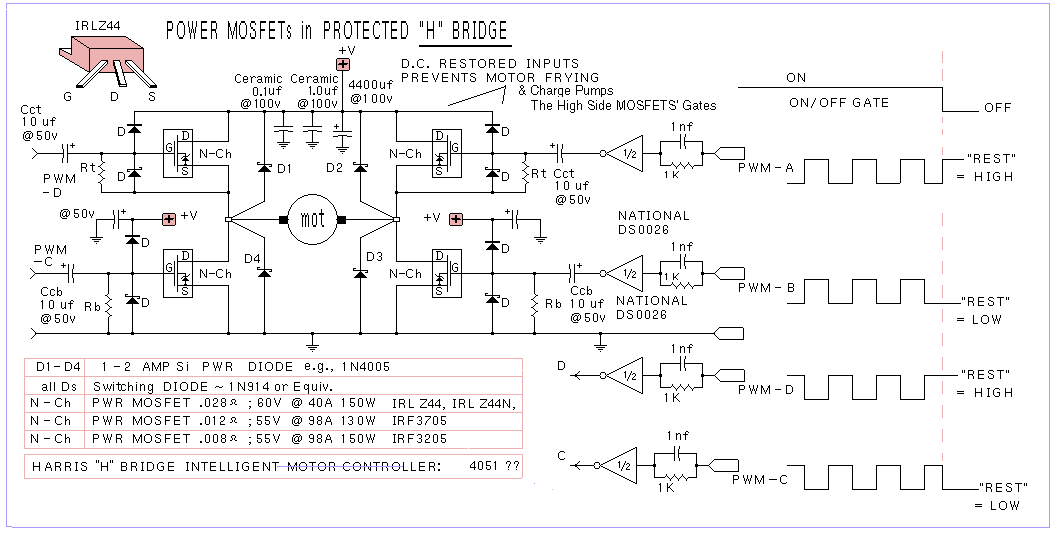
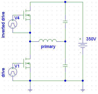
whats wrong my h bridge drivers

The H-bridge circuit is a critical component in driving motors and other inductive loads, allowing for bidirectional control of the load's direction and speed. In this scenario, the issue arises from the incorrect voltage levels observed at the output, which are expected to be a ±10V square wave but are instead presenting a constant 25V. This discrepancy suggests that the driving mechanism for the MOSFETs is not functioning as intended.
The complementary emitter configuration typically employs bipolar junction transistors (BJTs) to drive the gates of the MOSFETs. However, if the gates and sources of the MOSFETs are inadvertently connected, it can lead to improper gate drive signals, causing the MOSFETs to remain in a non-switching state. This situation can be exacerbated by the presence of multiple voltage sources, which may introduce complexity and confusion in the circuit design.
To rectify the gate drive issue, it is essential to ensure that the emitter followers are correctly biased. This requires providing sufficient voltage to the emitters to turn on the MOSFETs effectively. The suggestion to supply 50V plus 12V highlights the need for a proper gate drive voltage that exceeds the threshold voltage of the MOSFETs in use. If the gate voltage is insufficient, the MOSFETs will not switch on fully, leading to high resistance and excessive heat, potentially damaging the components.
For voltage translation, open-collector configurations with resistor pull-ups can be employed to achieve the desired voltage levels needed for driving the MOSFET gates. This method allows for level shifting while maintaining signal integrity. Additionally, AC coupling techniques can be advantageous in isolating the control signals from the load, preventing any feedback that could affect the operation of the circuit.
The recommendation to use ideal SPICE components is crucial for accurate simulation results. Ideal components eliminate parasitic elements that can skew results, providing a clearer understanding of the circuit's behavior. Removing unnecessary voltage sources, especially floating ones, will also simplify the schematic, making it easier to analyze and troubleshoot.
In conclusion, addressing the gate drive voltage, optimizing the schematic design, and utilizing appropriate components will lead to a more reliable and functional H-bridge circuit. Properly designed, this circuit can effectively drive motors with precise control over speed and direction.I`ve tried to make drivers for my H-bridge circuit using complimentary emmiters but the square wave outputs runat a constant 25v instead of +-10v square wave The image is a bit hard to read but it looks like your mosfets` gates and sources are wire together (or gate connection is missing). also you have 8 voltage sources - you might want to reduce that number. edit: you might want to make your schematic more compact, save at a higher resolution and crop out the unnecessary stuff (like anything but the schematic) the image is bigger and more readable. If you post the. ASC file for your circuit, I might play with it and see what I can come up with. You will have to either ZIP it, or change the extension to. TXT so that the forum will accept it. user1453, are you really sure the upper half of the H-bridge does what you think it does In order to turn the mosfet on, you`ll need to supply 50V + 12V to the emitter followers.
At present, Q3, Q4, Q7, Q8 are only ever going to see at most 12V. If this were a real circuit, those mosfets would`ve probably blown their gates - followed by some more smoke. Look up voltage translation circuits. Open-collector/resistor pull-up types are probably the kind you want, although AC coupling via capacitors/transformers would also do.
One side note - you`re probably also better off using as many "ideal" spice components as possible - AC voltage sources for the (I think it`s an oscillator, but I haven`t built any in a long time), and get rid of the voltage divider op-amp too. Also get of unnecessary voltage sources - especially floating ones- in the circuit. It makes it much harder to read and isn`t very realistic. 🔗 External reference
Related Circuits
The oscillator was designed to utilize resistors and capacitors instead of large low-frequency LC tank circuits for generating audio frequencies. It achieved low distortion (less than 0.5%) by employing a two-stage amplifier with sufficient negative feedback to set the...
Develop a cost-effective high-current circuit that utilizes PWM. The design includes flyback diodes to protect the MOSFET from the back EMF generated by the motor when the power is switched on and off via the PWM signal. This configuration...
The regenerative effect of a 4-quadrant inverter necessitates power dissipation in some form. In large industrial drives, this power is typically re-inverted back onto the national grid. However, for smaller applications, implementing a braking circuit is advisable. For low-power...
A very popular circuit for driving DC motors (ordinary or gearhead) is called an H-bridge. It's called that because it looks like the capital letter 'H' on classic schematics. The great ability of an H-bridge circuit is that the...
Which switch mode power supply (SMPS) topology should one start with? Although the schematic of a full-bridge looks a bit complicated compared to push-pull and half-bridge designs, sticking straight to a full-bridge topology or its smaller version, the half-bridge,...
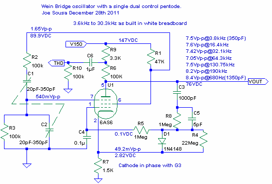
The classic Wien-Bridge oscillator, with incandescent lamp nonlinear stabilization, provides a low distortion sine wave source. A thorough and clear discussion of the Wien-Bridge oscillator is provided in Malvino's Electronic Principles. Using an inexpensive op-amp with sufficient bandwidth and...