
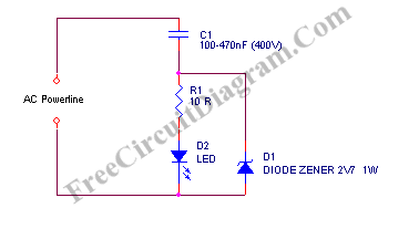
White LED Voltage Booster Uses 555 Timer IC

The circuit's design highlights the versatility of the 555 timer in low-voltage applications, particularly for driving LEDs. The astable multivibrator configuration allows for continuous operation with efficient energy transfer from the inductor to the LED. The choice of components such as the type of 555 timer, the values of resistors, and the specifications of the transistors directly influence the performance of the circuit. Careful selection of these components ensures that the circuit operates reliably under varying conditions, thus providing a practical solution for low-voltage LED applications. The implementation of feedback mechanisms and bootstrapping techniques enhances overall efficiency and performance, making this circuit an effective choice for hobbyists and engineers alike.This voltage-booster circuit for driving one or more white LEDs uses a 555 timer as its main element ( see the figure ). The timer, IC1, functions as a resettable astable multivibrator where R1, R2, and C2 are the timing components.
When the supply voltage, VS, is first applied, D1 conducts and reservoir capacitor C1 charges to a voltage just less than VS. Initially, transistor Q2 is off, IC1`s RESET input is high, and the OUTPUT pin goes high, allowing C2 to charge up via R1. During this time, the DISCHARGE pin is pulled up by R4, which turns on Q1, and the current (IL) in inductor L1 starts to ramp up.
Because Q1 is saturated, both D3 and the LED are reverse-biased. When the voltage on C2 crosses the threshold voltage at pin 6 of IC1, both the OUTPUT and DISCHARGE pins go low, and Q1 turns off. The resulting "back EMF" generated across L1 instantaneously raises the LED`s anode voltage (VA) above VS, thereby illuminating the LED.
Diode D3 is now forward-biased and pulls up IC1`s supply voltage (V+) to a level some 2 to 4 V higher than VS. C2 is now quickly discharged via D2 and R2, ready for the next cycle. Provided the values of R5 and R6 are chosen correctly, Q2 turns on while the LED is RESET input. When the energy stored in L1 is exhausted, the LED and D3 again become reverse-biased, and VA falls to a low level.
Q2 now turns off, allowing IC1 to commence another cycle, and C2 again begins to charge via R1. The process repeats thousands of times a second, so the LED appears to be continually illuminated. The circuit uses three "tricks" to optimize performance. First, the bootstrapping provided by D3 boosts the timer`s supply voltage, enabling the circuit to continue working even when VS drops below 1 V. In addition, it provides enhanced base drive for Q1 via R4. Second, the "feedback" provided via Q2 ensures that a new cycle begins as soon as L1`s energy is depleted, thereby maximizing the average LED current.
Third, Q1 is driven from the timer`s open-drain DISCHARGE terminal, rather than from the OUTPUT pin. Therefore, the base drive doesn`t depend on the current-source capabilities of the 555`s output terminal. where K is a constant that depends on the particular type of 555 timer used. The LED`s peak current is roughly equal to the maximum inductor current, IL(max), where: Thus, for a particular value of VS, the values of R1, C2, and L1 may be selected to obtain the largest value of IL(max) that produces maximum LED brightness without exceeding its peak current rating.
Resistors R5 and R6 should be chosen to ensure that Q2 is off when VA = VS (the case when power is first applied), and on when the LED is forward-biased (VA > VS). Q2 itself should be a small-signal device with good current gain. For efficient, low-voltage operation, a CMOS timer such as Intersil`s ICM7555 or Texas Instruments` TLC555 should be used.
These types are specified to function with a supply voltage as low as 2. 0 V. Plus, their internal discharge transistors are able to pull pin 7 down to around 100 mV or less, ensuring that Q1 can be turned fully off. A test circuit built using a TLC555 for IC1, and Q1 = ZTX649, Q2 = BC546, L1 = 100 µH, R5 = 56 k ©, and R6 = 10 k © was found to start up with VS as low as 1.
0 V. The circuit produced excellent brightness in a Lumileds ( ) LXHL-PW01 white LED. Transistor Q1`s "on" time (tON) was around 20 µs, resulting in a peak inductor current of around 300 mA at VS = 1. 5 V. However, this could easily be altered by changing the values of C2 and R1, and/or L1. Performance was equally impressive using an ICM7555, although the minimum startup voltage was slightly higher at 1.
2 V. The circuit is ideal for single-cell applications, because it continues to generate adequate LED intensity even when the supply voltage falls below 1. 0 V. Also, two or more LEDs may be connected in series, although there will be a corresponding reduction in brightness.
🔗 External reference
Related Circuits
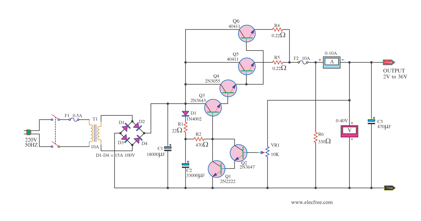
Yesterday, no enhancements were made to the circuit on the blog. Today, a high current power supply capable of delivering 10A has been introduced, featuring an adjustable voltage or variable voltage regulator that can operate within a range of...
The high durability of a light-emitting diode (LED) makes it suitable for ON/OFF indicator applications. However, there are limitations regarding low operating voltage. Light-emitting diodes (LEDs) are semiconductor devices that emit light when an electric current passes through them. Their...
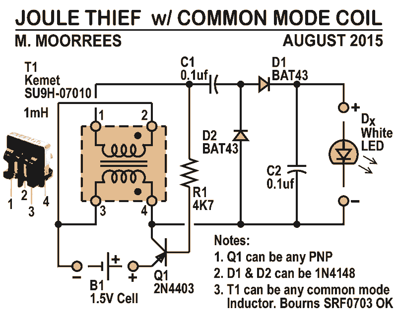
Like all joule thieves, this circuit boosts the voltage from a single 1.5V dry cell battery high enough to illuminate ultrabright GaN blue, green, or white LEDs. Instead of requiring a custom coil, it utilizes an off-the-shelf standard Kemet...
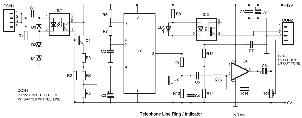
The circuit has been designed for telephone apparatus to indicate an incoming call as it rings using an LED for visual indication. BC550, an NPN general-purpose transistor, is utilized in the design. The circuit operates by detecting the ringing voltage...
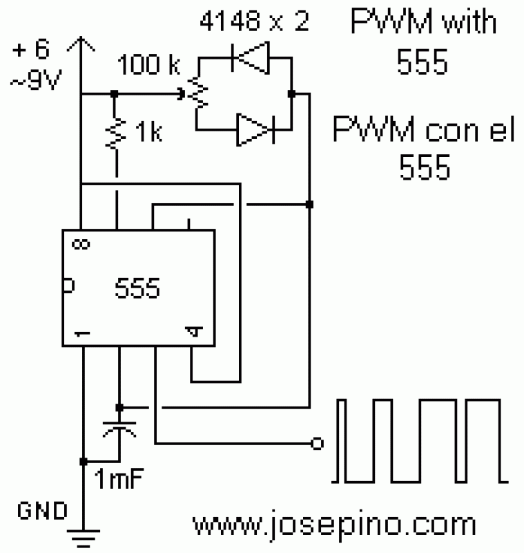
Pulse width modulation (PWM) is a technique to control analog circuits with a digital output. PWM is used in many applications, especially to control light intensity and speed on motors. A PWM circuit makes a square wave with a...
The parallel arrangement of LED backlights allows the control IC to utilize inexpensive low voltage CMOS processes, as illustrated in the following circuit diagram, which requires two to six white LEDs (WLEDs) in parallel. In many applications, LED backlights...
Warning: include(partials/cookie-banner.php): Failed to open stream: Permission denied in /var/www/html/nextgr/view-circuit.php on line 713
Warning: include(): Failed opening 'partials/cookie-banner.php' for inclusion (include_path='.:/usr/share/php') in /var/www/html/nextgr/view-circuit.php on line 713