
Wide band differential multiplexer
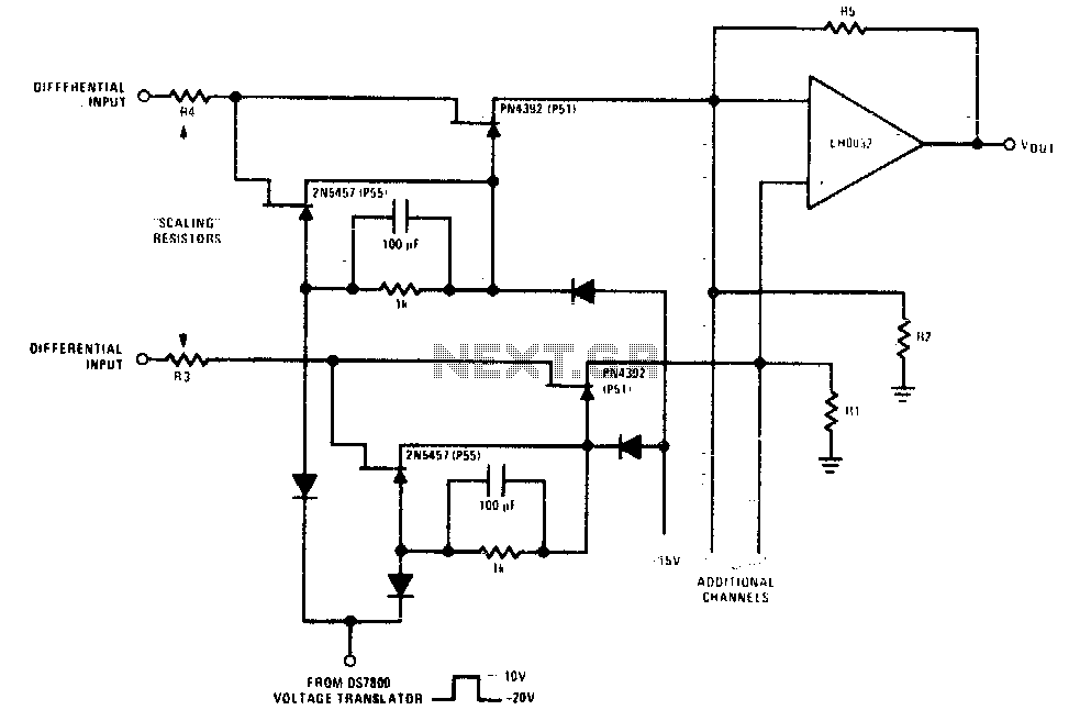
The circuit is designed to manage high-frequency signals effectively while maintaining rapid toggle rates, making it suitable for applications requiring quick signal processing and switching. The architecture typically employs high-speed transistors or operational amplifiers that can operate efficiently at frequencies reaching several megahertz.
In practical applications, this circuit can be utilized in digital communication systems, where data rates demand swift transitions between high and low states. The ability to toggle at rates up to 1 MHz ensures that the circuit can accommodate various modulation schemes, enhancing overall system performance.
To achieve the desired toggle rates, careful attention must be paid to the circuit layout, including minimizing parasitic capacitance and inductance, which can adversely affect performance at high frequencies. Components such as low-capacitance FETs or high-speed bipolar transistors are often selected to ensure rapid switching times and reliable operation.
Additionally, the circuit may incorporate feedback mechanisms to stabilize performance under varying load conditions, which is crucial for maintaining signal integrity. Proper decoupling of power supply lines and grounding techniques should also be implemented to reduce noise and improve the overall reliability of high-frequency operations.
Overall, this circuit design represents a robust solution for applications where both high-frequency signal processing and rapid switching capabilities are essential.This design allows high frequency signal handling and high toggle rates simultaneously Toggle rates up to 1 MHz and MHz signals are possible with this circuit. 🔗 External reference
Related Circuits
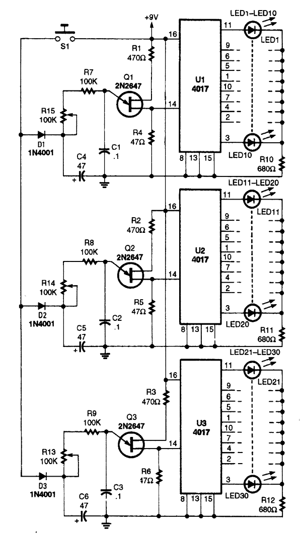
The one-arm bandit circuit consists of three clock circuits and three counter/readout circuits. A single roll switch, S1, activates all three clocks simultaneously. When S1 is closed, capacitors C4, C5, and C6 charge through diodes D31, D32, and D33...
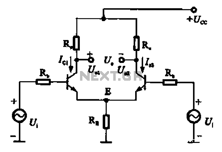
The common mode signal of an emitter-coupled differential amplifier circuit assumes that two equal small increases of the same polarity signal, referred to as the common mode signal, occur simultaneously. This results in an increase in the potential at...

The following diagram illustrates the circuit of a 20-band stereo graphic equalizer designed to control audio signals within specific frequency ranges. This circuit should be connected prior to the amplifier circuit to ensure optimal performance. The 20-band stereo graphic equalizer...
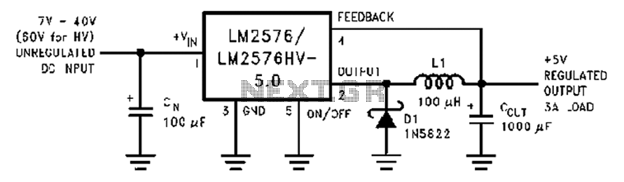
A wide range of 7 to 40V DC-DC step-down circuit that converts input voltage to 5V. This circuit operates as a buck converter, designed to efficiently reduce a higher DC voltage (ranging from 7V to 40V) to a stable output...
The CXA1821M is an integrated circuit designed for compact disc players. This IC includes an Automatic Power Control (APC) circuit along with RF, focus error, and tracking error amplifiers for 3-spot optical pickup output. It also supports voltage-converted optical...
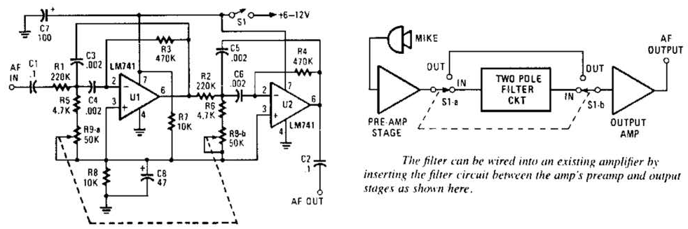
This variable-frequency audio bandpass filter is constructed using two 741 operational amplifiers connected in cascade. The two 741 op amps are configured as identical RC active filters and are cascaded to enhance selectivity. The filter's tuning range spans from...