
Wien bridge oscillator
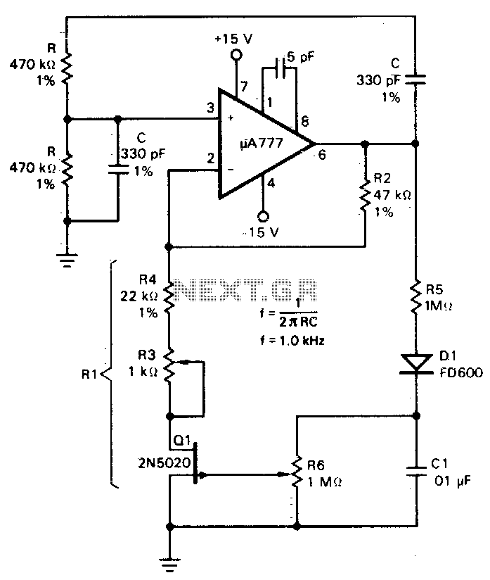
The circuit design incorporates a field effect transistor (FET) as a critical component in achieving automatic gain control. The operation of the FET in the linear resistive region is vital for maintaining stable oscillation conditions. The RC network's attenuation characteristic is specifically tuned to one-third at the zero phase-shift oscillation frequency. This tuning is crucial as it dictates that the gain of the amplifier, defined by the relationship between resistors R2 and R1, must equal three. This ratio ensures that the positive feedback loop achieves unity gain, which is a prerequisite for stable oscillatory behavior.
Resistors R3 and R4 are strategically selected to be approximately 1000 ohms less than the target resistance of R1. This selection allows for fine-tuning of the gain control mechanism, providing a buffer within the circuit's operational parameters. The FET plays a significant role in dynamically adjusting the resistance value of R1, allowing it to be half the value of R2. This dynamic adjustment is essential for maintaining the desired gain characteristics of the circuit.
Moreover, the circuit segment consisting of R5, D1, and C1 is designed for signal processing. It effectively isolates the output sine wave generated by the oscillation, rectifying and filtering it to produce a stable DC voltage. This DC potential is then utilized to control the gate of the FET, ensuring that the device operates within its optimal parameters. The low drain-to-source voltages employed in this configuration enable the FET to provide a symmetrical linear resistance, which is advantageous for achieving consistent performance in response to varying gate-to-source voltage levels. This design approach highlights the sophistication and precision required in analog circuit design, particularly in applications involving automatic gain control and oscillatory systems.Field effect transistor, Ql, operates in the linear resistive region to provide automatic gain control. Because the attenuation of the RC network is one-third at the zero phase-shift oscillation frequency, the amplifier gain determined by resistor R2 and equivalent resistor R1 must be just equal to three to make up the unity gain positive feedback requirement needed for stable oscillation.
Resistors R3 and R4 are set to approximately 1000 ohm less than the required R1 resistance. The FET dynamically provides the trimming resistance needed to make R1 one-half of the resistance of R2 The circuit composed of R5, Dl, and CI isolates, rectifies, and filters the output sine wave, converting it into, a dc potential to control the gate of the FET. For the low drain-to-source voltages used, the FET provides a symmetrical linear resistance for a given gate-to-source voltage.
🔗 External reference
Related Circuits

This circuit is a voltage-controlled oscillator (VCO) that utilizes the 555 timer integrated circuit (IC) as its primary component. The 555 timer is configured as an astable multivibrator, enabling it to function as an oscillator. An astable multivibrator is...
A voltage-controlled oscillator is an oscillator whose frequency of oscillation can be varied by changing an applied voltage. A voltage-controlled oscillator (VCO) is an essential component in various electronic systems, particularly in communication devices, signal processing, and modulation applications. The...
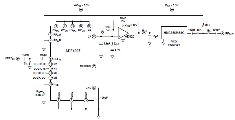
The ADF4007 high-frequency divider Phase-Locked Loop (PLL) synthesizer can be utilized in a variety of communication applications. It operates up to 7.5 GHz on the RF side and 120 MHz at the Phase Frequency Detector (PFD). The device includes...
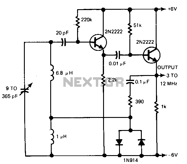
The gain control enables the oscillator to maintain a nearly constant output across its range. The circuit operates within a frequency range of 160 kHz to 12 MHz while producing a consistent amplitude. The oscillator circuit described utilizes a gain...
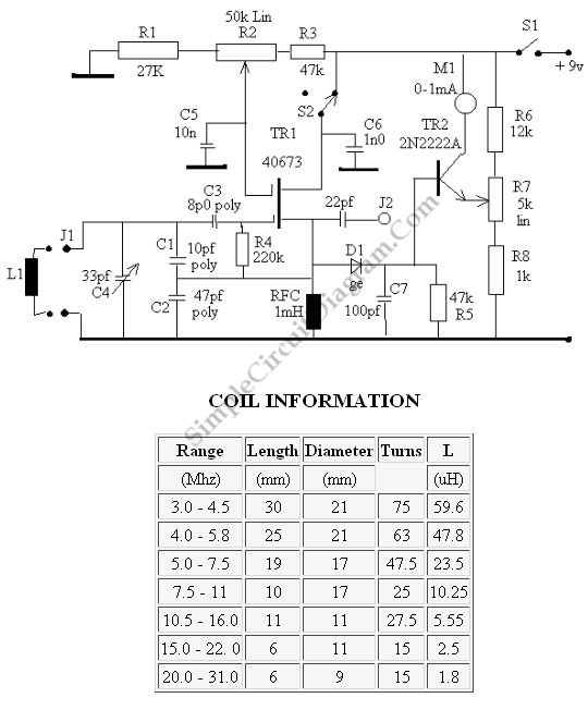
This is a grid dip oscillator (GDO) circuit developed by Luigi Falcone. The circuit uses seven plug-in coils that cover the frequency range of 3.0 to 30 MHz. It can be connected to a frequency meter through the coaxial...
The Oscillator Design Guide is integrated into Agilent EEsof's Advanced Design System environment, functioning as a smart library and interactive handbook for the creation of effective designs. It facilitates quick oscillator design, interactive component characterization, and provides in-depth insights...