
Wireless Interface RF Modules Circuit

The schematic comprises two primary RF modules, one for transmission and the other for reception, operating on a shared power supply derived from a regulated +5V output. The LM7805 voltage regulator is a linear voltage regulator that efficiently converts higher battery voltages to a stable +5V, which is essential for the reliable operation of the RF modules and microcontrollers. The inclusion of a DC filtering capacitor serves to smooth out any voltage fluctuations and noise, ensuring that the RF modules receive clean power, which is critical for maintaining signal integrity.
The RF transmitter module is responsible for encoding and sending data wirelessly, while the RF receiver module decodes the incoming signals. The microcontrollers, 18F452 and 18F4520, are programmed to manage the data flow between the transmitter and receiver, utilizing the designated TX and RX pins for communication. The TX pin (PORTC 6) sends data from the microcontroller to the transmitter module, which modulates the data onto a carrier wave for transmission. Conversely, the RX pin (PORTC 7) receives the modulated signal from the receiver module, which demodulates the signal back into a format that the microcontroller can process.
The design emphasizes minimizing data transmission errors, which is crucial in RF communication. The use of the respective data pins ensures that the microcontrollers can effectively control the data flow, while the RF modules handle the wireless communication. Future modifications to the receiver module may include error correction techniques to further enhance the reliability of the data transmission, addressing potential distortions that may occur during the wireless transfer. This comprehensive approach facilitates robust communication between the two circuits, making it suitable for various applications in wireless data transmission.The RF modules used in this schematic are very simple, with only a few extra pins required for power, ground and data. The main parts used in this schematic are the RF transmitter module, RF receiver module, 18F452 and 18F4520.
You can see them below, as well as the specific circuits described in more detail. Since there are two seperate circu its, both need to have a power supply circuit. The power supply in both circuits is identical, a LM7805 takes battery input and regulates it down to +5v. The DC filtering capacitor cleans up any noise off the +5v output. The only difference for this part of the circuit is that the receiver uses the RX pin (PORTC 7) on the PIC and the transmitter uses the TX pin (PORTC 6) on the PIC.
Both of these data lines connect to the data pin on the transmitter or receiver module. These two modules are in charge of passing the data from one link to the other without adding too much error. We`ll see later in the theory section how the receiver module can be altered to help correct distortion.
🔗 External reference
Related Circuits
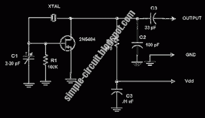
This circuit is a conventional Pierce-type oscillator that utilizes a JFET. It operates with fundamental mode crystals, offering decent performance and reliability when a low noise JFET is employed. The feedback is regulated by the capacitance of C1 from...
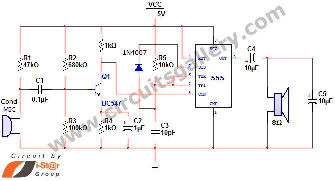
This document discusses a simple project utilizing the 555 timer IC. The 555 timer IC can be configured as an audio amplifier using an astable multivibrator configuration. It performs pulse width modulation (PWM) on an audio signal. The current...
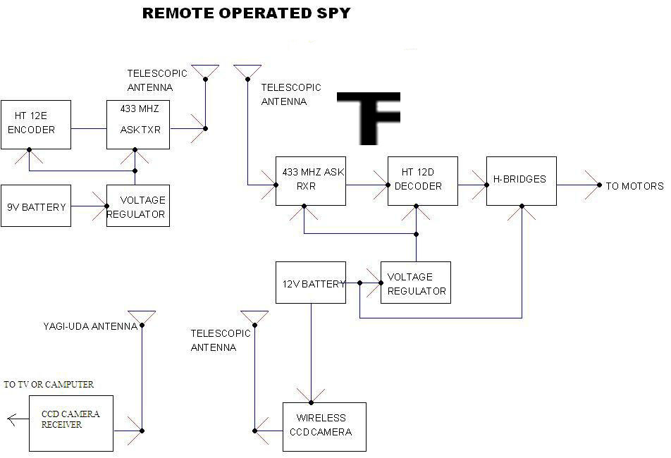
A robot that operates when you send messages through your phone. Your mobile device serves as the remote controller for the robot. This means that if the robot is in London and you are in Mumbai, you can still...
This application note discusses the use of SEPIC power modules to supply the necessary power for driving high-brightness LED arrays. These arrays serve as display backlights and necessitate a wide dimming range. The SEPIC configuration offers an efficient and...
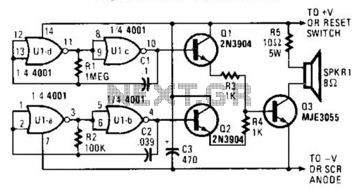
An external horn-type speaker is optimal for this circuit. However, such devices demand significant power, so this sounder should only be employed in alarm circuits utilizing at least a 6-A SCR as the sounder driver. The circuit incorporates a...
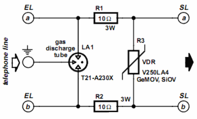
A long time ago, when telephones were simple and reliable from an electrical standpoint, telecom operators installed surge protection on all telephone lines at risk from storms. Paradoxically, as modern technology has led to the use of delicate and...