
XTR108 reverse voltage and overvoltage protection circuit diagrams
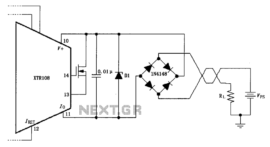
The circuit design incorporates a Zener diode configured to limit the voltage across sensitive components, ensuring that any voltage exceeding the specified threshold is clamped to a safe level. The Zener diode operates in reverse breakdown mode, where it maintains a constant output voltage even as the input voltage varies, thus providing reliable overvoltage protection.
In conjunction with the Zener diode, a diode rectifier bridge is employed to safeguard against reverse voltage conditions. This bridge consists of four diodes arranged in a configuration that allows current to flow in one direction while blocking reverse current, protecting the circuit from potential damage caused by incorrect polarity.
It is essential to consider the voltage drop across the diodes in the rectifier bridge, which typically amounts to approximately 1.4V for silicon diodes. This voltage drop must be factored into the circuit design, as it dictates that the supply voltage (VPS) should remain below the Zener diode's minimum breakdown voltage to avoid exceeding its limits and risking component failure.
In summary, the circuit effectively combines Zener diode overvoltage protection with a diode rectifier bridge to ensure robust performance and reliability, while careful attention to voltage specifications is critical for optimal operation. As shown, the circuit uses a zener diode D1 achieve overvoltage protection, a diode rectifier bridge to achieve reverse voltage protection. Diodes 1.4V loop will cause the maxi mum loss of voltage VPS must be lower than the minimum zener diode breakdown voltage.
Related Circuits
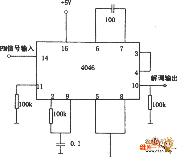
The FM demodulator circuit, as illustrated in the figure, utilizes a 4046 Phase-Locked Loop (PLL) integrated circuit to convert the intermediate frequency FM input signal into a lower frequency output. The FM demodulator circuit based on the 4046 PLL IC...
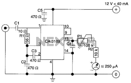
The design of the digital logic probe centers around a pair of complementary bipolar transistors, which, in this application, are used as electronic switches. The digital logic probe is a diagnostic tool utilized for testing and analyzing digital circuits. The...
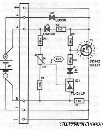
This voltage regulator for devices that utilize solar cells is straightforward and requires only a few electronic components. When a rechargeable energy storage device is employed, the voltage regulator circuit facilitates charging when the output voltage of the cell...
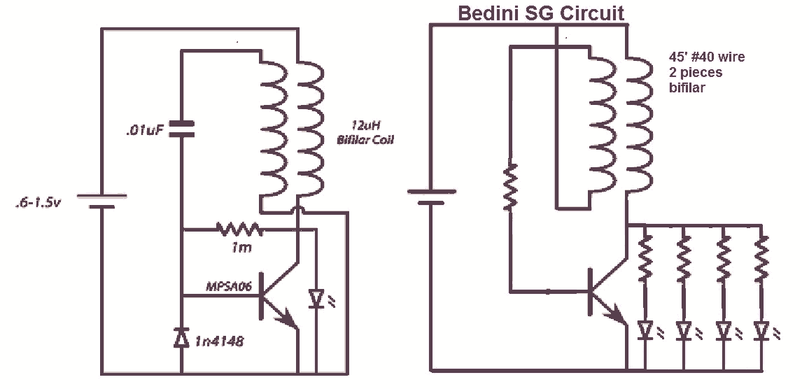
It would be beneficial to obtain schematics of the Joule Thief and Bedini oscillator circuit connections. This is an area that has not been previously explored. The schematic on the left was sourced from the Energetic Forum, while the...
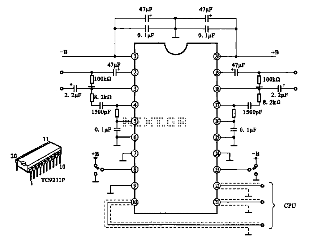
A typical electronic volume control circuit is commonly used in stereo audio devices connected through a computer (CPU). The circuit adjusts the volume of stereo signals via input and output pins. Control signals are sent to the CPU (including...
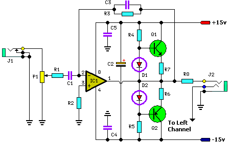
In addition to its primary function as a headphone amplifier, the circuit is suitable for various applications requiring a wide bandwidth low power amplifier. It is constructed using an operational amplifier (op-amp), with its output current enhanced by a...