
Simple Digital Logic Probe Circuit
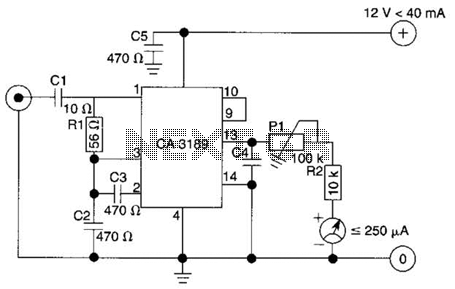
The digital logic probe is a diagnostic tool utilized for testing and analyzing digital circuits. The core of its design involves two complementary bipolar transistors, typically an NPN and a PNP type, configured to operate as electronic switches. This configuration allows for the detection of high and low logic levels in a circuit, facilitating the identification of signal states.
When a voltage is applied to the base of the NPN transistor, it turns on, allowing current to flow from the collector to the emitter. Conversely, when the PNP transistor is activated, it allows current to flow in the opposite direction. This complementary action ensures that the probe can effectively toggle between detecting logic high (1) and logic low (0) states.
The output of the probe can be connected to an LED indicator or a microcontroller input, providing a visual or digital representation of the logic state. Additional components, such as pull-up or pull-down resistors, may be included in the circuit to stabilize the input signals and prevent floating states.
In summary, the digital logic probe serves as an essential tool in electronic testing, leveraging the properties of complementary bipolar transistors to provide accurate readings of digital signals in various applications. The design of the digital logic probe centers around a pair of complementary bipolar transistors, which, in this application, are used as electronic switches. 🔗 External reference
Related Circuits
This solid-state push-pull single-ended Class A circuit is capable of providing sound quality comparable to that of valve amplifiers. It delivers an output power of 6.9W when measured across an 8 Ohm loudspeaker cabinet load, with reduced total harmonic...

The hum noise is produced by an electronic device with improper design. To address this issue, it is essential to identify the source of the hum. This involves checking the grounding, cabling, casing, and other factors that may contribute...
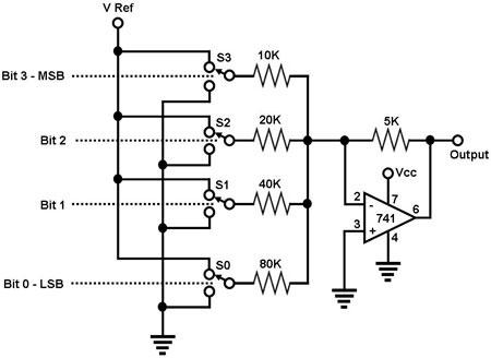
The circuit depicted in Figure 1 is a straightforward 4-bit digital-to-analog converter (DAC). It functions as a simple operational amplifier (op-amp) summer circuit, configured to produce an output voltage that is proportional to the sum of the input voltages....
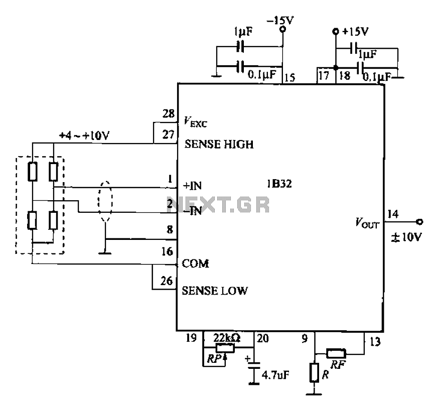
The circuit for bridge measurements is straightforward, as illustrated in the figure. The sensor bridge drive voltage can be adjusted between +4V and +10V, depending on the specific requirements of the sensor. Two fixed gain options of 333.3 and...

The power is measured by the circuit AD8307 over a 50 ohm dummy load. An A/D converter of 12 bit converts the analog output from the AD8307 to a digital number. Since the AD is a 12 bit A/D,...
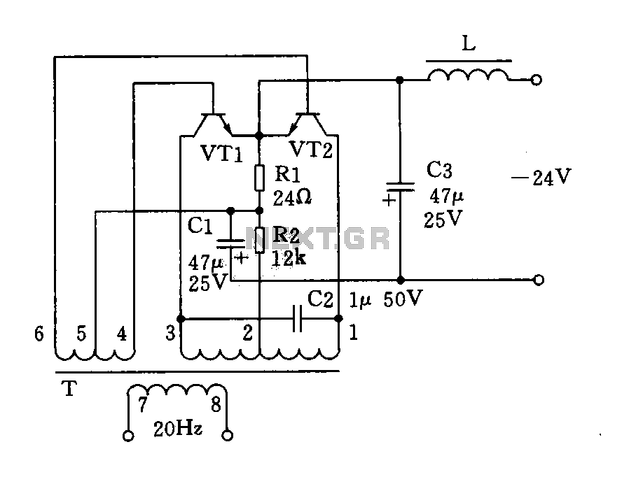
The circuit described is a 20Hz signal generator suitable for telephone ringing systems, alarm systems, and various other electronic applications. It consists of a transformer (T) and two transistors (VT1 and VT2), forming a push-pull oscillator. The two transistors...