
XTR112 114 bridge input current excitation circuit diagram
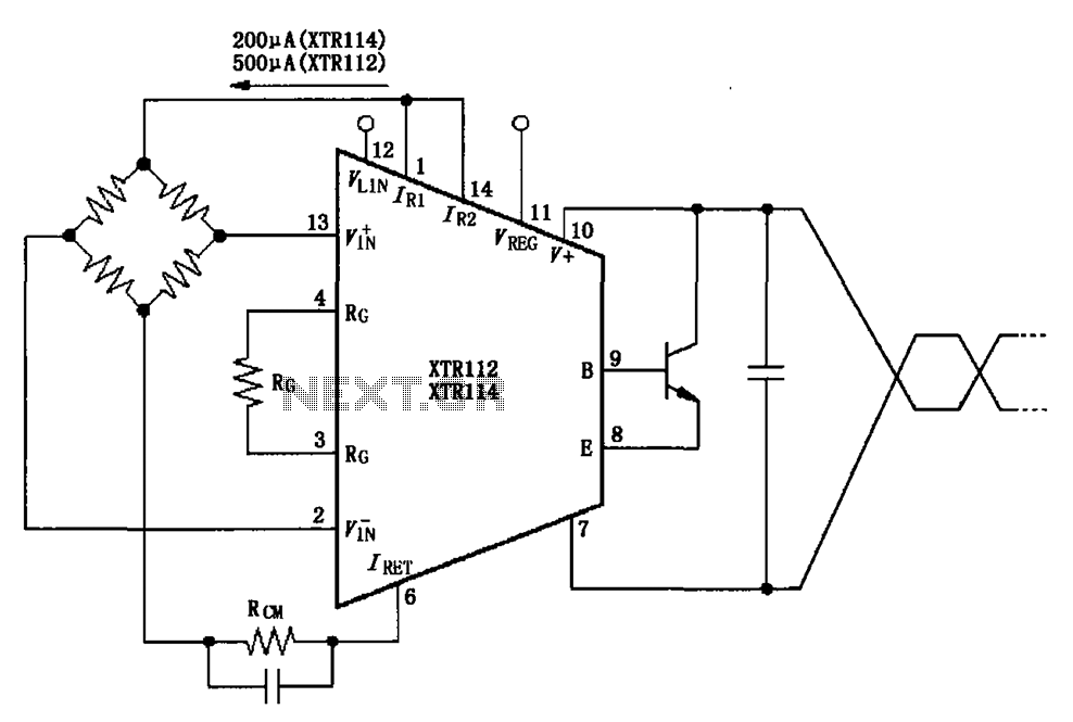
The circuit features two distinct current sources designed to deliver precise excitation levels for various applications. The XTR114 current source outputs a nominal current of 0.2 mA, while the XTR112 is capable of providing a higher output of 0.5 A. This versatility allows for adaptability in different circuit configurations, depending on the required current specifications.
The adjustment of the common mode input voltage is a critical aspect of this design, allowing it to be finely tuned within a range of 1.25 V to 3.5 V. This feature enhances the circuit's performance by accommodating variations in the input signal conditions, thus ensuring stable operation under diverse scenarios.
In practical applications, these current sources can be utilized in sensor interfaces, signal conditioning, or as part of a larger analog system where precise current regulation is necessary. The ability to bridge excitation with adjustable common mode voltage ensures that the circuit can maintain optimal performance across a variety of environmental and operational conditions.
Overall, the integration of these current sources within a single chip simplifies design processes and enhances reliability, making it a valuable component in modern electronic systems. As shown, the two current sources inside the chip (1 foot and 14 feet out) bridge excitation, the output of each current source is 0.2mA (XTR114) or 0.5A (XTR112). With RCM adj usted common mode input voltage, so that is 1.25 ~ 3.5V.
Related Circuits

Operating at approximately 1.1 GHz, the detector senses disturbances in the electromagnetic field surrounding the antenna. The Doppler signal generated by detector D1 is amplified and used to control a power MOSFET switch. The antenna consists of a short...
This circuit turns off an amplifier or any other device when it remains idle for 15 minutes. It is powered by the amplifier's tape output. The described circuit functions as an automatic power management system, designed to enhance energy efficiency...
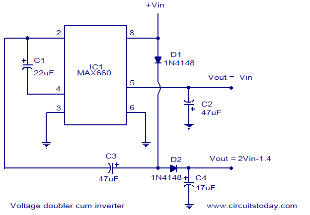
Voltage doubler circuit and voltage inverter circuit diagram with schematics using MAX660 IC, which is a DC voltage multiplier IC. This is a DC voltage doubler circuit and inverter. The MAX660 integrated circuit (IC) is designed for applications requiring a...
The BC547 transistor has a maximum operating current of 100 mA and a maximum voltage rating of 65 volts. When oriented with the label facing the viewer, the three terminals from left to right are collector, base, and emitter....
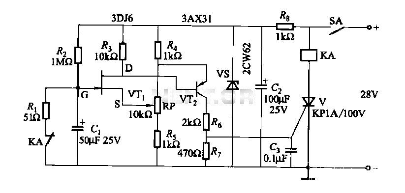
FET relay circuit 2 is essentially a JS-20 time relay circuit. When the switch SA is open, the relay device KA remains in the released state. Once switch SA is closed, the delay period begins. After a specified duration,...

The circuit diagram of the device features a 555 timer IC configured as a transmitter and a receiver, divided into two sections. The 555 timer in the transmitter section serves as the core component of a frequency oscillator. The...
Warning: include(partials/cookie-banner.php): Failed to open stream: Permission denied in /var/www/html/nextgr/view-circuit.php on line 713
Warning: include(): Failed opening 'partials/cookie-banner.php' for inclusion (include_path='.:/usr/share/php') in /var/www/html/nextgr/view-circuit.php on line 713