
Zero Feedback Impedance Amplifiers
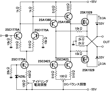
The amplifier under discussion features a simplified design that maintains high performance while reducing the number of components required for assembly. This can lead to easier troubleshooting, lower manufacturing costs, and potentially improved reliability.
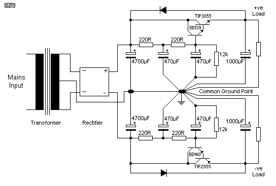
Key components typically include operational amplifiers, resistors, capacitors, and transistors, arranged in a configuration that optimizes signal amplification. The schematic may show a power supply stage, input stage, and output stage, with each section designed to handle specific tasks such as filtering, gain adjustment, and output drive.
The power supply section is crucial, as it provides the necessary voltage and current to the amplifier. It may involve a transformer, rectifier, and smoothing capacitors to ensure a stable DC supply.
The input stage usually consists of a differential amplifier configuration to minimize noise and improve signal integrity. This stage might include input coupling capacitors to block DC offsets while allowing AC signals to pass through.
The gain stage amplifies the input signal, typically using a combination of transistors and feedback resistors to set the gain level. This stage must be carefully designed to avoid distortion and maintain linearity across the desired frequency range.
Lastly, the output stage is responsible for driving the load, which could be a speaker or another circuit. It may employ a push-pull configuration to enhance efficiency and reduce heat generation.
In summary, this amplifier design, with its lower parts count, is not only feasible but also advantageous for those looking to build an efficient and effective audio amplification solution.Dear Susan, your amp is similar to this one which has even a lower parts number. It deserves to be built!.. 🔗 External reference
Related Circuits
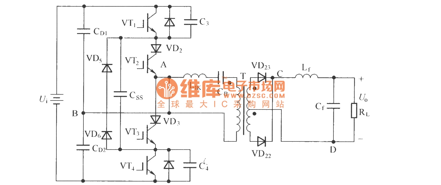
To eliminate circulating current in a zero-voltage switch three-level DC converter during its zero state, a zero-voltage zero-current switch three-level DC converter circuit has been proposed. The primary distinction between this circuit and the standard zero-voltage switch three-level DC...
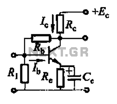
Basic reference transistor bias circuit - Mixed Negative feedback The basic reference transistor bias circuit utilizing mixed negative feedback is a fundamental electronic configuration designed to stabilize the operating point of a transistor. This circuit typically employs a combination of...
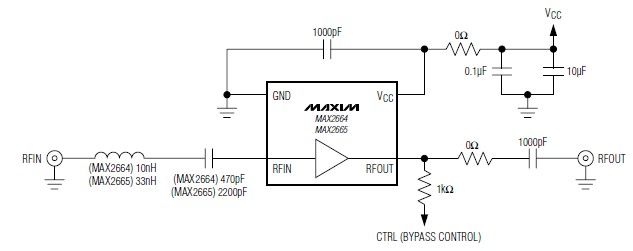
These devices feature a broadband low-noise amplifier (LNA) with an integrated bypass switch. The MAX2664 operates within the UHF frequency range of 470 MHz to 860 MHz, while the MAX2665 functions within the VHF frequency range of 75 MHz...
Since I have provided the schematic for John L Linsley-Hood's Class-A amplifier, I felt that some readers may wish to experiment with the concept. Unfortunately, a very low ripple power supply is needed for all Class-A amps, and the...
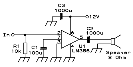
Approximately one watt RMS appears to be a suitable output level, which is also the maximum power that a basic amplifier powered by 12V can deliver to an 8 Ohm speaker. A very low saturation amplifier may reach up...
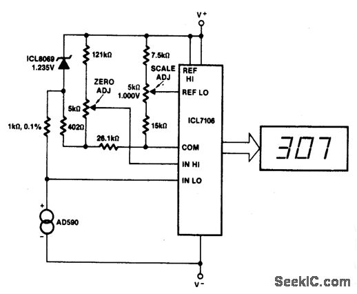
This circuit allows for zero adjustment as well as slope adjustment. The ICL8069 brings the input within the common-mode range, while the 5 K pots trim any offset at 218 °K (-55 °F) and set the scale factor. The...