
LM4910 minimum output noise reduce the output power circuit

The LM4910 circuit configuration aims to enhance audio performance by minimizing noise and optimizing power efficiency. The series resistor connected to the output terminal serves as a low-pass filter, effectively reducing the amplitude of unwanted noise signals that may interfere with the desired audio output. The choice of resistance value is critical, as it directly influences the attenuation level of the output noise.
The feedback resistor Rf is paired with a bypass capacitor Cf to form a high-frequency noise suppression network. This configuration allows for the filtering of high-frequency components that could degrade audio quality. The capacitor Cf should be selected based on the desired cutoff frequency, ensuring effective suppression of noise while maintaining the integrity of the audio signal.
The inclusion of jumper J1 provides flexibility in power management. In shutdown mode, the amplifier's power consumption is significantly reduced, which is beneficial in battery-operated devices where energy efficiency is paramount. The transition from shutdown to active mode is controlled by the state of jumper J1; when connected to ground, the amplifier is disabled, and when left open, it operates at full capacity. The maximum power output of the amplifier is calculated using the formula PDMAX = 4VDD²/2RL, where VDD is the supply voltage and RL is the load resistance. This relationship highlights the importance of selecting appropriate values for both VDD and RL to achieve optimal performance from the LM4910 amplifier. As shown for the LM4910 minimum output noise/reduce the output power circuit. Reduce output noise measures are: between the output terminal of a resistor in series with the loa d Rseries, so that the output noise can be attenuated, to achieve the purpose of reducing noise; in parallel across the feedback resistor Rf frequency bypass capacitor Cf, with to suppress high frequency noise. J1 short jumper, when short jumper J1 is grounded, the amplifier is in shutdown mode, the power consumption to a minimum; when J1 short jumper off (VDD high), the amplifier is in working mode, the power PDMAX 4VDD2/2RL.
Related Circuits
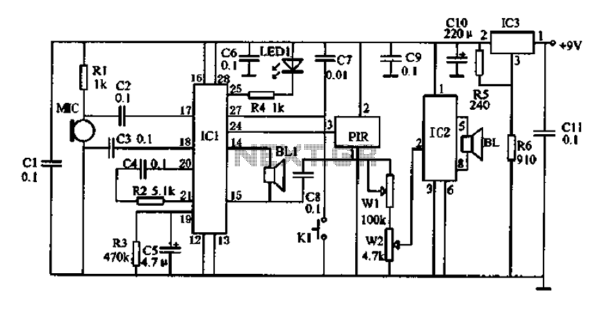
Doppler effect sensor N1 (RD627), operational amplifier N2 (LM358), and a special integrated circuit for imitating dog barking (N3, KD5608) are utilized along with other components. When there is no activity detected in the monitoring area by N1, the...
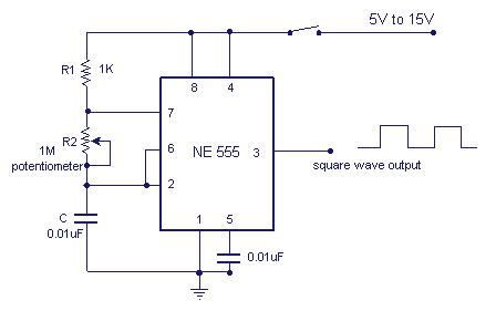
A NE555 integrated circuit (IC) is utilized for the design of a variable low-frequency oscillator, and a schematic is provided. The NE555 timer IC is a versatile and widely used device in various electronic applications, particularly in generating precise timing...

The circuit is capable of driving the company's Dialight 745-0005 monitor, which features a 64-character alphanumeric display. It generates 0-second and 1-second input signals on lines A1 through A6 based on the phase response of the desired characters, utilizing...
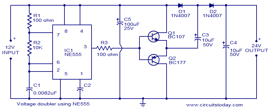
This circuit demonstrates a voltage doubler utilizing the NE555 timer. It is a straightforward project. The NE555 integrated circuit is configured as an astable multivibrator. The NE555 timer is a versatile component commonly used in various electronic applications, including timing,...
Cellular phone detector circuit schematic using common electronic parts The cellular phone detector circuit is designed to identify the presence of a cellular phone within a specified range. This circuit utilizes basic electronic components, making it accessible for hobbyists and...
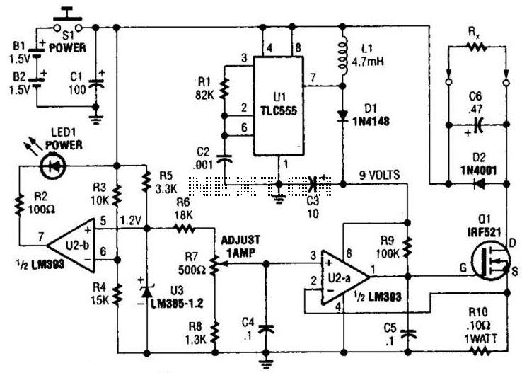
Useful for low-resistance measurements, this 1-A current source will produce 1 A in unknown resistance Rx. For best results, Rc should be less than 1 to 2, because only 3 V are available. Ul is a flyback converter to...