
0-50V 1A power supply with CA3086

This power supply circuit is designed to maintain a highly stable output voltage across a wide range of load conditions and input voltage fluctuations. The circuit features an operational amplifier (opamp) CA3130, which plays a critical role in voltage regulation. The opamp compares the reference voltage, generated by a temperature-compensated transistor array (IC1), to the output voltage. This arrangement ensures minimal voltage drop (0.005%) under varying load conditions from 0% to 100%.
The reference voltage is established through a potentiometer (P1), allowing for fine-tuning of the output voltage, which can be adjusted from 0.1V to 50V. The temperature-compensated array consists of five transistors, with four functioning as reference diodes and the fifth controlling the output impedance, providing stable performance over temperature variations.
The opamp's output is connected to a voltage divider, which scales down the output voltage before it is fed into the non-inverting input of the opamp. This feedback mechanism is essential for achieving precise voltage regulation. The circuit incorporates a Darlington pair configuration using transistors T1 and T2, which enhances current amplification, ensuring that the output can handle significant loads.
Transistor T3 serves as a current limiter, providing protection against overcurrent conditions. The current limit is adjustable via the potentiometer P1, with a minimum threshold of 0.6 amperes. When P1 is set to its maximum position, the current limiting feature is effectively disabled, allowing for maximum current delivery to the load.
Transistor T4 is employed to elevate the output voltage while isolating the opamp from the higher voltage levels present at the output. This isolation is crucial for protecting the sensitive components of the circuit while maintaining operational integrity.
Overall, this power supply circuit exemplifies advanced design principles in voltage regulation and current limiting, making it suitable for applications requiring high stability and adaptability in output voltage across varying conditions.This power supply circuit is highly stabilized that its output voltage will drop only 0.005% even though the load changes from 0 to 100%. Another excellent capability is that the output voltage will change only by 0.01% if the input voltage fluctuates.
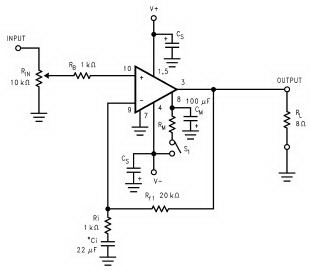
The capability if the circuit to be adjusted from 0.1V up to 50V is due to the application of opamp IC CA3130 in the circuit. Transistor T4 raises the output voltage to higher level, and at the same time it separates the lower level opamp from the high level of the output voltage.
The reference voltage is supplied by IC1. It is a temperature compensated transistor array with 5 transistors. Four of these transistors are used as reference diodes and the fifth one sets the output impedance of the reference source. The reference voltage is set through P1. The opamp CA3130 compares the reference voltage at its minus input to the output voltage at its input.
The output voltage passes first through a voltage divider before it is fed into the plus input of the opamp. Transistors T1 and T2 work as darlington pair and amplifies the current. Transistor T3 functions as current limiter. The current limit is ajustable through P1, and the lowest current limit is 0.6 ampere. Once potentiometer P1 is set at maximum, current limiting is disabled. 🔗 External reference
Related Circuits
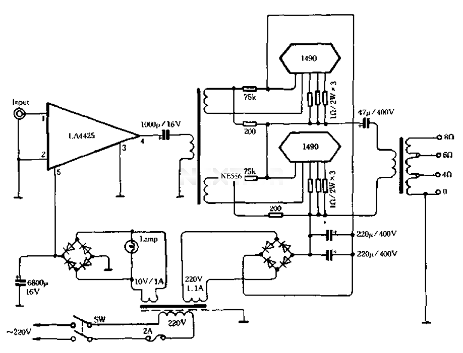
As illustrated in Figure 3-30, the IC LA4425 power amplifier stage is utilized alongside a pair of power module 1490 configured for push-pull output. This setup functions as an impedance converter, enabling the system to deliver 100 watts of...

The LM317 is capable of providing extremely good load regulation, but a few precautions are needed to obtain maximum performance. For best performance, the programming resistor (R1) should be connected as close to the regulator as possible to minimize...
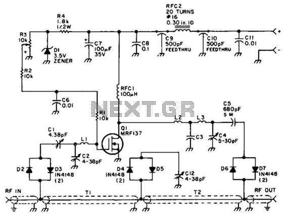
Using a power MOSFET, this amplifier can achieve a 2-W handheld radio power level, increasing it to approximately 10 W on the 2-meter band. A transmission-line RF switch is employed for transmit/receive (T/R) switching. The described amplifier utilizes a power...
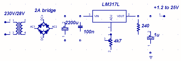
A truly timeless circuit. LM317 is a versatile and highly efficient 1.2-37V voltage regulator that can provide up to 1.5A of current with a large heat sink. It's ideal for just about any application. Since LM317 is protected against...
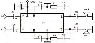
This series utilizes the TDA2822M integrated circuit (IC) as the primary amplifier. Additionally, alternative ICs such as KA2209, NJM2073, U2822B, and U2823B can be employed alongside the TDA2822M. The output power is limited to a maximum of 4 watts,...
The Audio Power Amplifier is a crucial component in sound reproduction within audio systems. The LM3886 Audio Power Amplifier is a highly capable integrated circuit that can deliver 68 Watts of power with a 4 Ohm load and 38...