
0-90 phase shifter circuit diagram

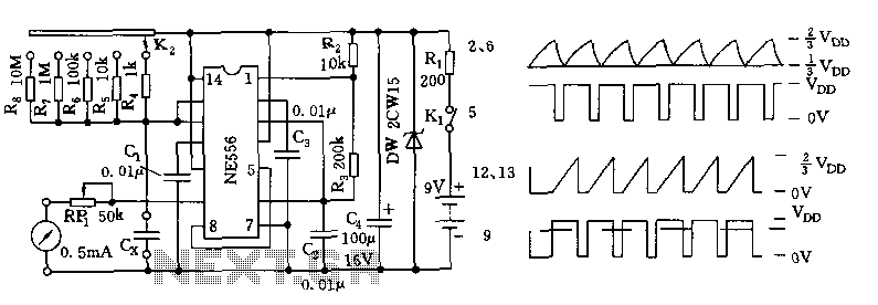
The application of automatic plotters in measuring the capacitance-voltage characteristics of solar Schottky gate diodes involves a systematic approach to analyzing the behavior of these diodes under varying electrical conditions. The measurement setup includes a diode connected in a specific configuration that is detailed in the accompanying schematic. The integrated circuit (IC) utilized in this setup produces a square wave output, which is essential for driving the measurement process.
Resistor R3 plays a critical role in the circuit, as its adjustable value, ranging from 0 to 90 ohms, facilitates the continuous modulation of the input signal. This adjustment is crucial for observing how the capacitance characteristics of the Schottky diode respond to different voltage levels. The ramp circuit designed for this application is integral to achieving accurate measurements, as it generates the necessary voltage sweep to characterize the diode's behavior effectively.
The design equations associated with the ramp circuit are vital for understanding the operational parameters of the measurement system. These equations provide insights into the relationship between the various components, including the effects of resistance, capacitance, and the frequency of the square wave output. By applying these design principles, engineers can optimize the circuit for enhanced performance and reliability in measuring the capacitance-voltage characteristics of solar Schottky gate diodes.Application of automatic plotters for measuring solar Schottky gate capacitance - voltage characteristics. Measured diode connected as shown below. IC square wave output phase, you can adjust R3, from 0 to 90 constantly shift. This paper presents the ramp circuit and design equations.
Related Circuits
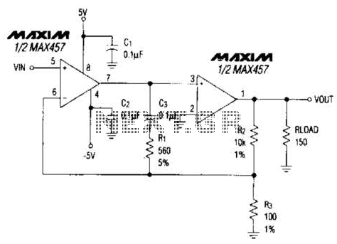
A composite amplifier can be constructed that offers high gain, wide bandwidth, and good DC accuracy by cascading the sections of a dual video amplifier and incorporating two suitable phase compensation components. The operational amplifier drives a 150-ohm load...
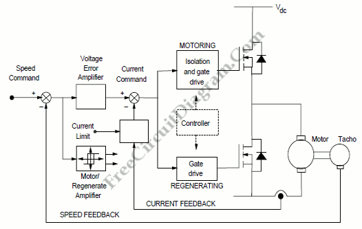
A schematic arrangement for a two-quadrant controller is shown in the figure below. This figure illustrates the outer speed control loop and the inner current control loop. The tachogenerator derives the speed feedback signal; alternatively, an approximation of the...
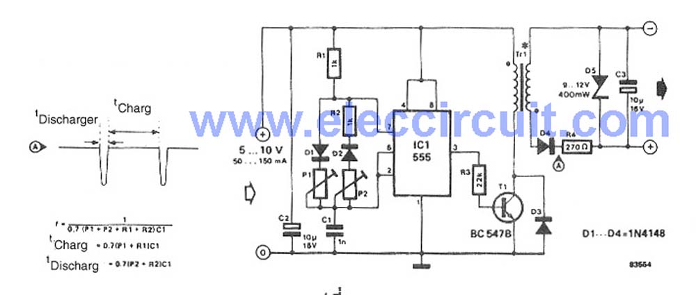
This circuit is a simple DC to DC converter designed for digital circuits. It operates with a supply voltage of 5V and provides an output voltage that steps up to a maximum of 10V-12V DC. The circuit utilizes an...

This section provides guidance on avoiding common issues with charts, diagrams, and other graphic representations. Engineers frequently utilize diagrams; however, while a detailed schematic diagram on a lab bench may accurately depict the work, it could present excessive information...
The tester comprises a dual time base circuit using a 556 timer and various RC components. The right side of the circuit features the 556 timer (556 1/2) along with resistors R2, R3, capacitors C2, C3, and additional components...
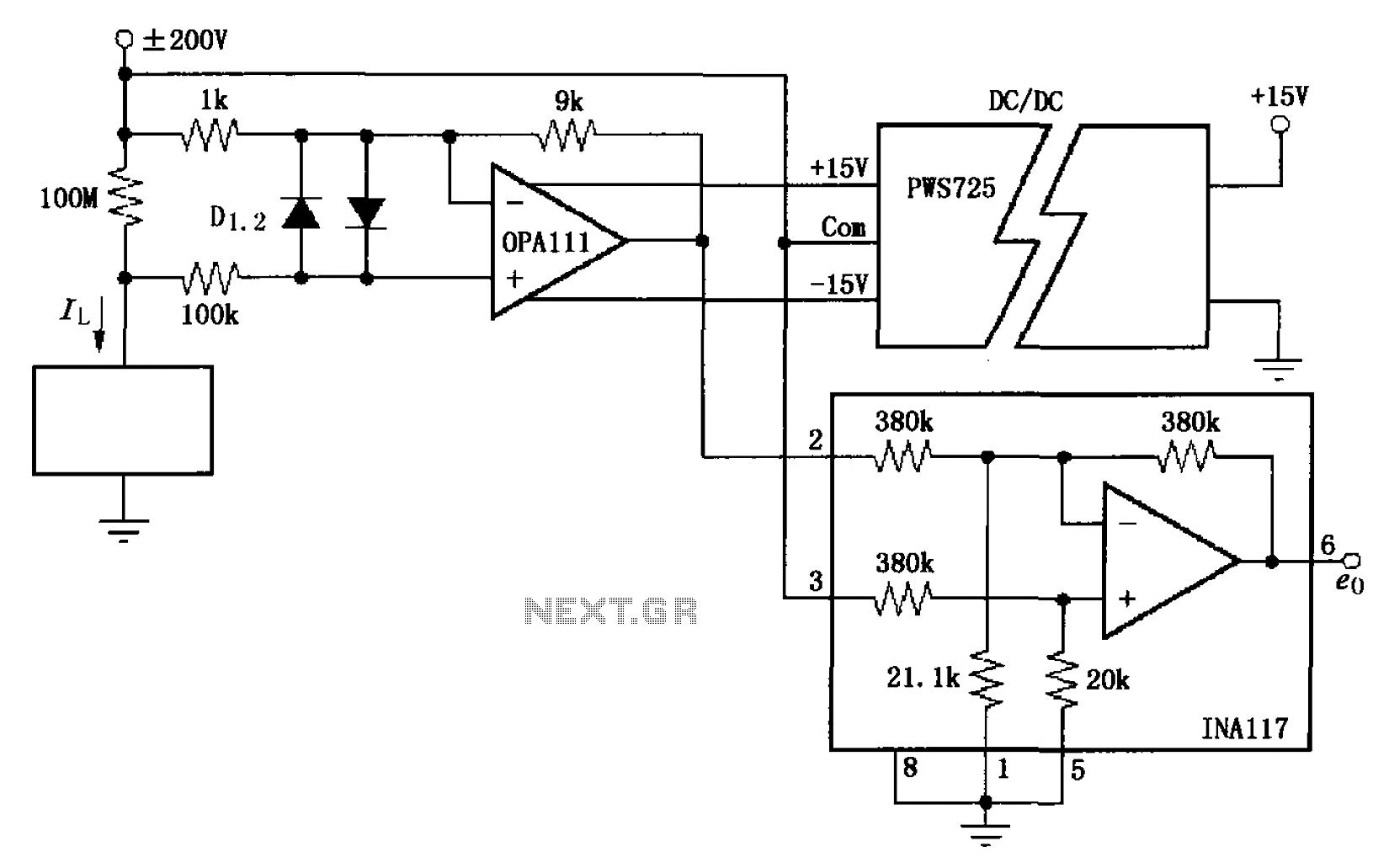
The circuit illustrated in FIG OPA111 is designed for measuring input buffer leakage current. The transistors D1 and D2, which are 2N3904 types, short the base and collector contacts while leaving the emitter open. When a power supply of...