
0 to 10V output multiplexer measuring circuit

The 1832 low drift input circuit is designed for high-precision applications where minimal temperature drift and excellent linearity are critical. The temperature coefficient of 0.07 µV/°C ensures that the output remains stable across varying temperature conditions, making it suitable for sensitive transducer applications. The linearity specification of 0.005% maximum indicates that the output signal closely follows the input signal without significant distortion, which is essential for accurate measurements.
The circuit's capability to drive resistive loads greater than 120 ohms is particularly important for bridge excitation applications, where the sensor's output must be sufficiently strong to provide reliable data. The output voltage range of +4 to +15 V allows for flexibility in interfacing with various transducer types, while the built-in oscillator and filter enhance signal integrity by reducing noise and unwanted frequency components.
The output drift of only 40 ppm/°C is indicative of the circuit's high stability, which is vital for precision signal conditioning in bridge transducer systems. The inclusion of two fixed gain settings (333.3 and 500) along with adjustable gain pins provides versatility in scaling the output signal to match the requirements of different applications, accommodating a wide range of input signal amplitudes from 100 to 5000.
The specified output voltage of 10 V is optimal for many data acquisition systems, ensuring compatibility with standard analog input ranges. The operating supply voltage range of 12 to 18 V allows for integration with various power supply configurations, making the 1832 low drift input circuit a robust choice for engineers designing high-performance measurement systems.1832 low drift input 0. 07pr, V/oC (RTI, G 500), excellent linearity (maximum 0.005%), can drive resistive loads greater than 120fl bridge excitation circuit (output + 4 ~ + 15 V) with osc, filter circuit, output drift only precision bridge transducer signal conditioning circuit 40ppm/of. At the same time, also set up 333.3,500 two fixed gain 100 to 5000 pins and gain adjustment pins. Output voltage is 10V. Operating supply voltage range of (12 ~ 18) V.
Related Circuits
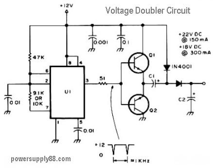
This circuit diagram represents a DC voltage doubler and DC converter. It is designed to convert a 12V DC power supply into outputs of 24V DC and 18V DC. Nearly any PNP or NPN power transistors can be utilized...
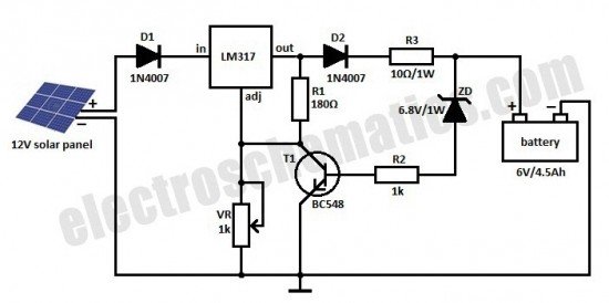
This is a solar charger circuit designed to charge Lead Acid or Ni-Cd batteries using solar energy. The circuit captures solar energy to charge the batteries. The solar charger circuit typically consists of several key components, including a solar panel,...
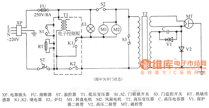
XP power plug, FU fuse, ST temperature control, T1 low-voltage transformers, S1, S2 door interlock switch, S3 threshold control switch, RT thermal sensor, K1, K2 relay, EL furnace light, M1 wheel motor, M2 fan motor, T2 high-voltage transformer, C...
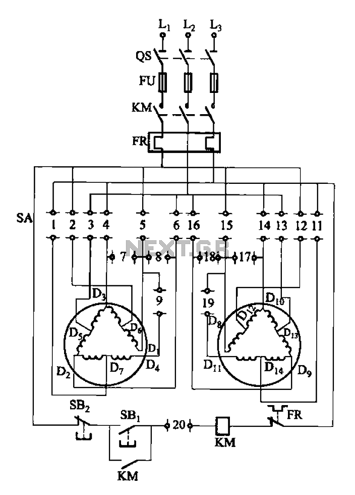
The 3-119 circuit shown in the figure combines switch SA to realize the stator windings, specifically the 2, Y, and 2Y connections, which correspond to the motor speed n1. The 3-119 circuit is designed to facilitate the control of motor...
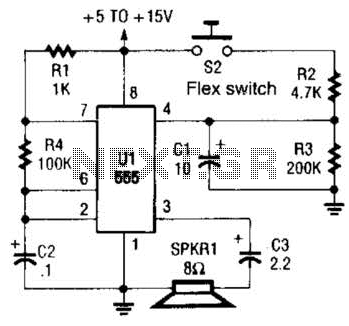
This is a cross-sectional diagram of a flex switch. They can be used as pushbuttons or even position sensors. This schematic diagram shows an oscillator, which is used as an alarm sounder, triggered by a flex switch. The flex switch...
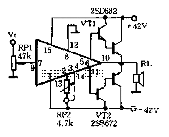
The AP500A amplifier offers numerous advantages, providing unmatched superiority in stereo applications. It can utilize various amplifier configurations, including OTI, CI, rK, BTL, class AB, and super CP. The typical DC amplifier module for the AP500A is illustrated in...