
10w 225-400mhz linear amplifier

A compensation network consisting of Rl, Cl, and LI enhances the input Voltage Standing Wave Ratio (VSWR) and stabilizes the gain response of the amplifier. The base bias choke is constructed from L2 and a small ferrite bead. The output network features a microstrip L-section comprising Z3 and C7, along with a high-pass section formed by C8 and L3. C8 also serves as a DC blocking capacitor. Collector decoupling is achieved using components L4, L5, C9, C10, Cll, C12, and C13.
This broadband amplifier circuit is engineered for military communication applications, specifically targeting the 225-400 MHz frequency range. The design focuses on achieving a high output power of 10 watts while maintaining efficient operation from a 28-volt power supply. The integration of a 50-ohm source and load ensures optimal power transfer and minimizes signal reflections, crucial for maintaining signal integrity in communication systems.
The input matching network, composed of capacitors and a transmission line, is designed to match the amplifier's input impedance to the 50-ohm source, facilitating effective signal coupling. The DC blocking capacitor (C2) is critical for preventing DC voltage from affecting the preceding stages of the circuit while allowing RF signals to pass through.
The compensation network (Rl, Cl, and LI) plays a vital role in improving the input VSWR, which is essential for minimizing signal loss and distortion. By flattening the gain response across the operating bandwidth, the amplifier can provide consistent performance, which is particularly important in military communication applications where reliability is paramount.
The output network, featuring a microstrip L-section and a high-pass filter, is designed to ensure that the output signal is within the desired frequency range while attenuating unwanted lower frequency signals. The inclusion of a DC blocking capacitor (C8) at the output stage further protects downstream components from DC voltage.
Collector decoupling is implemented through a series of inductors and capacitors (L4, L5, C9, C10, Cll, C12, and C13) to stabilize the supply voltage and minimize noise, ensuring that the amplifier operates efficiently and reliably under varying load conditions. This comprehensive design approach results in a robust broadband amplifier suitable for demanding military communication environments.This broadband amplifier covers the 225-400 MHz military communications band producing 10 watt RF output power and operating from a 28 volt supply. The amplifier can be used as a driver for higher power devices such as 2N6439 and MRF327. The circuit is designed to be driven by a 50 ohm source and operate into a nominal 50 ohm load. The input matching network consists of a section composed of C3, C4, Z2, C5 and C6. C2 is a dc blocking capacitor, and Tl is a 4:1 impedance ratio coaxial transformer. Z1 is a 50 ohm transmission line. A compensation network consisting of Rl, Cl, and LI is used to improve the input VSWR and flatten the gain response of the amplifier. L2 and a small ferrite bead make up the base bias choke. The output network is made up of a microstrip L-section consisting of Z3 and C7, and a high pass section consisting of C8 and L3.
C8 also serves as a dc blocking capacitor. Collector decoupling is accomplished through the use of L4, L5, C9, C10, Cll, C12, and C13.
Related Circuits

The power used for realignment is considered a loss in the context of the overall circuit. Due to the hysteresis loss in the saturable-core reactor, the power gain is relatively low. Adding a rectifier to the load circuit can...
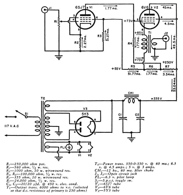
A Direct-Coupled 6V6 Tube Amplifier with Cathode Follower by Raymond H. Bates from Radio & Television News magazine, November 1949. The Direct-Coupled 6V6 Tube Amplifier is designed to utilize a 6V6 vacuum tube, which is known for its warm sound...
The circuit illustrates a simple method for adjusting the high input impedance of a double wave linear detector. It employs an operational amplifier configured with a negative feedback loop to compensate for the non-linear behavior of the diode used...

A very high-power amplifier with 10 pairs of power transistors. It can utilize MJ15024 and MJ15025 or MJ21193 and MJ21194. These 20 transistors function as the final active components. The design is based on four integrated circuits: TL072, TL074,...
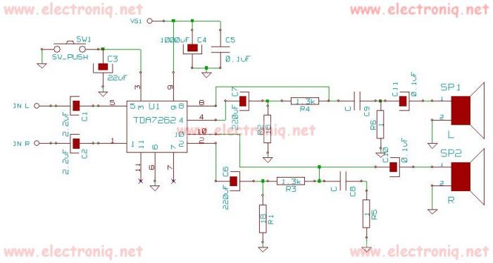
TDA7262 stereo 20 watts audio amplifier circuit design electronic project The TDA7262 is an integrated circuit designed for stereo audio amplification, capable of delivering up to 20 watts per channel. This amplifier circuit is suitable for various applications, including home...
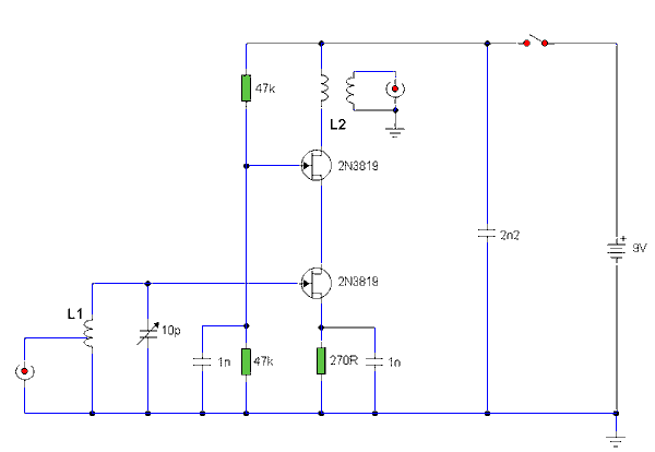
The circuit utilizes two 2N3819 FETs configured in a cascode arrangement. The lower FET functions in common source mode, while the upper FET operates in common gate mode, achieving full high-frequency gain. The lower FET is tunable, enabling peak...